Insertion of repeaters without timing constraints

a repeater and wire technology, applied in repeater circuits, line-transmission details, instruments, etc., can solve the problems of all design technology areas hitting a brick wall, affecting the continuation of the industry's historical success, and affecting the timing performance of the net, so as to boost the timing performance and boost the timing performance

Inactive Publication Date: 2006-03-07
CADENCE DESIGN SYST INC
View PDF6 Cites 22 Cited by
  • Summary
  • Abstract
  • Description
  • Claims
  • Application Information

AI Technical Summary

Benefits of technology

[0018]In one embodiment, the present invention is embodied as a method of inserting buffers in a circuit design, comprising the steps of, preparing a physical hierarchy of the circuit design with placed macros, performing global routing on the physical hierarchy, determining a number of buffers to be inserted on each edge of nets of the global routing for boosting timing performance of the nets, calculating a position for each buffer, and inserting a buffer configured to boost timing performance at each calculated position.

Problems solved by technology

The NTRS report concluded that the industry is rapidly approaching a formidable “100 nm barrier” that threatens the continuation of the historical success the industry has enjoyed.
The most alarming finding of this working group was that the industry has become very “idea limited,” and almost all areas of design technology would hit a brick wall by the year 2006, when the industry anticipates the first shipment of 100 nm technology.
However, it has become very clear that even if the various components of a design automation toolset could handle specific issues in their respective domain, the overall problems of size, diversity and productivity may not he solved unless a coherent and comprehensive approach to tools working together in a convergent flow is taken.
Also, for “deep sub-micron” (DSM) manufacturing processes (i.e. those less than or equal to 0.18 micron), the problem of wire delay becomes a significant issue.
Prior to DSM, most of the delay on a chip was due to the logic gates, and the delay associated with the wires was relatively insignificant.
The problem of wire delay dominance can cause serious problems for standard prior art design techniques.
Modern designs having 10 million or more transistors are simply too large for current design tools to handle, so the designs are broken down in manageable blocks.
After the process is complete, certain wires will be too long (i.e. too much delay), so the whole process must be repeated.
However, as a result of the re-design some other wires now have too much delay.
This problem is known in the industry as the “timing convergence” problem.
At several weeks per iteration, the design cycle time is a significant factor in the cost and delay in the design and implementation of a chip.
When the wire delays actually become dominant for DSM designs, the timing convergence problem is seriously exacerbated.

Method used


Image

  • Insertion of repeaters without timing constraints
  • Insertion of repeaters without timing constraints
  • Insertion of repeaters without timing constraints

Examples


Embodiment Construction

[0029]The following description is provided to enable any person skilled in the art to make and use the invention and sets forth the best modes contemplated by the inventor for carrying out the invention. Various modifications, however, will remain readily apparent to those skilled in the art, since the basic principles of the present invention have been defined herein specifically to provide a method of inserting repeaters in integrated circuit wires, without timing constraints. Any and all such modifications, equivalents and alternatives are intended to fall within the spirit and scope of the present invention.

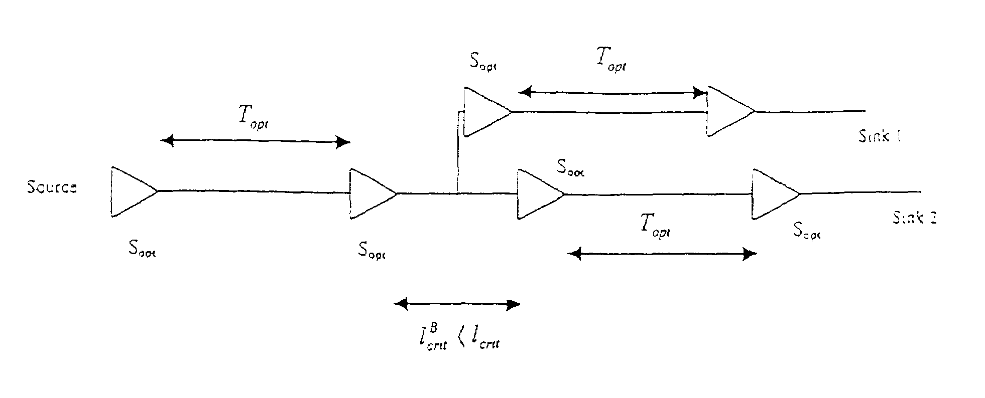
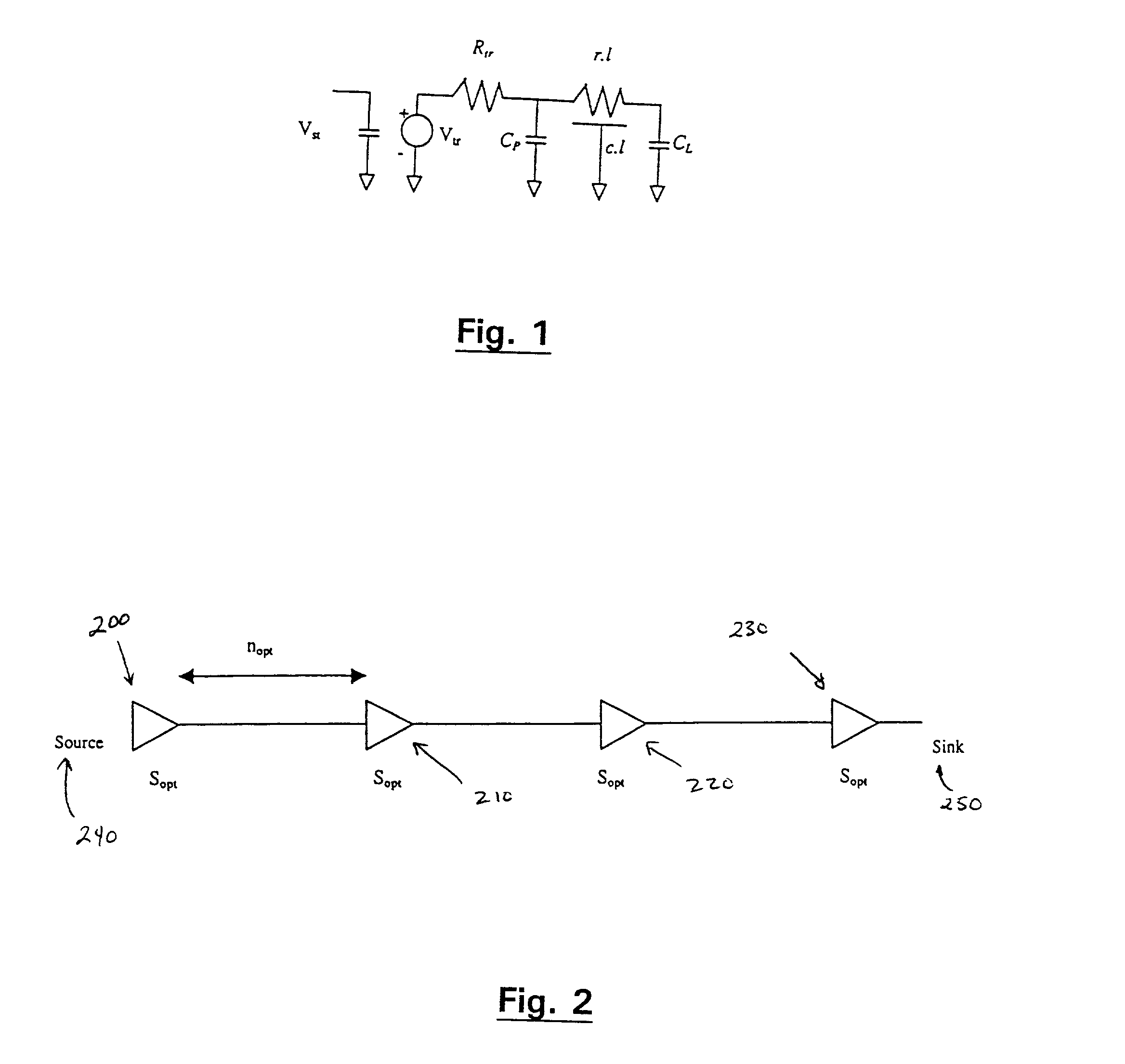
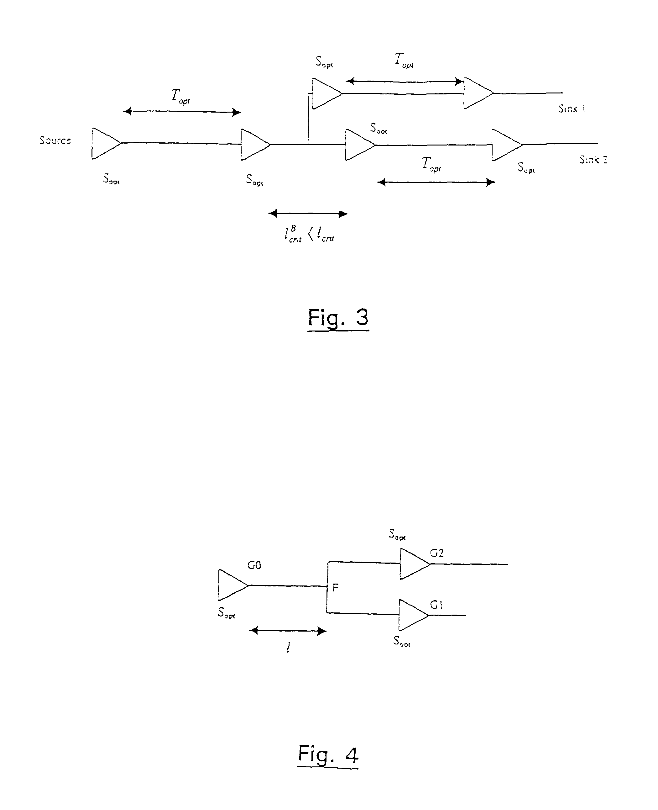
[0030]In general, the present invention relates to speeding up electrical signals in integrated circuit chips to either improve performance of the chips and / or to alleviate timing violation problems. The design of today's chips involves many iterations in order to get closure on the timing constraint problem. This is due to the lack of tight coupling between the logic synthe...


PUM


Abstract

A method/process for repeater insertion in the absence of timing constraints. Delays are optimized for multi-receiver and multi-layer nets and can be introduced in the early steps of design planning. It serves as a tool for interconnect prediction as well as planning. In the presented formulation, no restrictions are made on where the repeaters are added or what the topology of the net is. The tabulated results demonstrate improvement (speed ups) using the method/process of the present invention. The present invention runs in linear time and achieves better results that the existing dynamic programming formulation and other published heuristics. Polarity in a circuit design is corrected by traversing the circuit and carrying backwards a cost of fixing the polarity. On a subsequent traversal, buffers inserted fix the polarity.

Description

CROSS REFERENCE TO RELATED APPLICATIONS AND CLAIM OF PRIORITY[0001]This invention claims priority to the following co-pending U.S. provisional patent application, which is incorporated herein by reference, in its entirety:[0002]Saldanha et al, Provisional Application Ser. No. 60 / 245,334, entitled “System Chip Synthesis,” attorney docket no. 21891.02100, filed, Nov. 1, 2000.BACKGROUND OF THE INVENTION[0003]1. Field of Invention[0004]The present invention relates generally to the field of integrated circuits, and more particularly to a method of inserting repeaters into integrated circuit wires without timing constraints.[0005]2. Discussion of Background[0006]The Semiconductor Industry Association's (SIA) 1997 National Technology Roadmap for Semiconductors (NTRS) (www.scmichips.org) looked at the challenges the semiconductor industry would have to overcome in order to sustain the rapid technology development it has enjoyed in the past several years. The NTRS report concluded that the ...

Claims


Application Information

Patent Timeline
Patent Type & Authority Patents(United States)
IPC IPC(8): G06F17/50H04B3/36
CPCG06F17/5072G06F17/505G06F30/327G06F30/392G06F2119/12G06F30/3947
Inventor ELASSAAD, SHAUKISALDANHA, ALEXANDER
Owner CADENCE DESIGN SYST INC
Why Eureka
Try Eureka