Magnetic memory cell with plural read transistors

a transistor and magnetic memory technology, applied in the field of solid-state memory, can solve the problems of excessive current and/or power usage, excessive heat generation,

Active Publication Date: 2006-03-14
MICRON TECH INC +1
View PDF6 Cites 161 Cited by
  • Summary
  • Abstract
  • Description
  • Claims
  • Application Information

AI Technical Summary

Problems solved by technology

Insufficient MR compared to required voltage levels could lead to errors,

Method used


Image

  • Magnetic memory cell with plural read transistors
  • Magnetic memory cell with plural read transistors
  • Magnetic memory cell with plural read transistors

Examples


Embodiment Construction

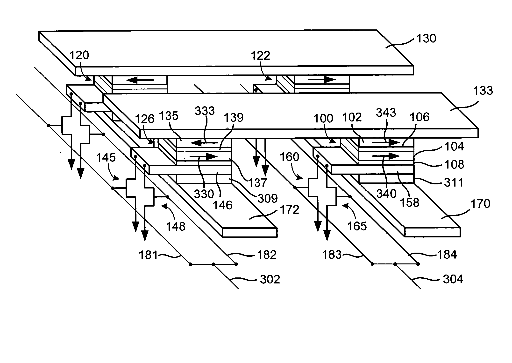
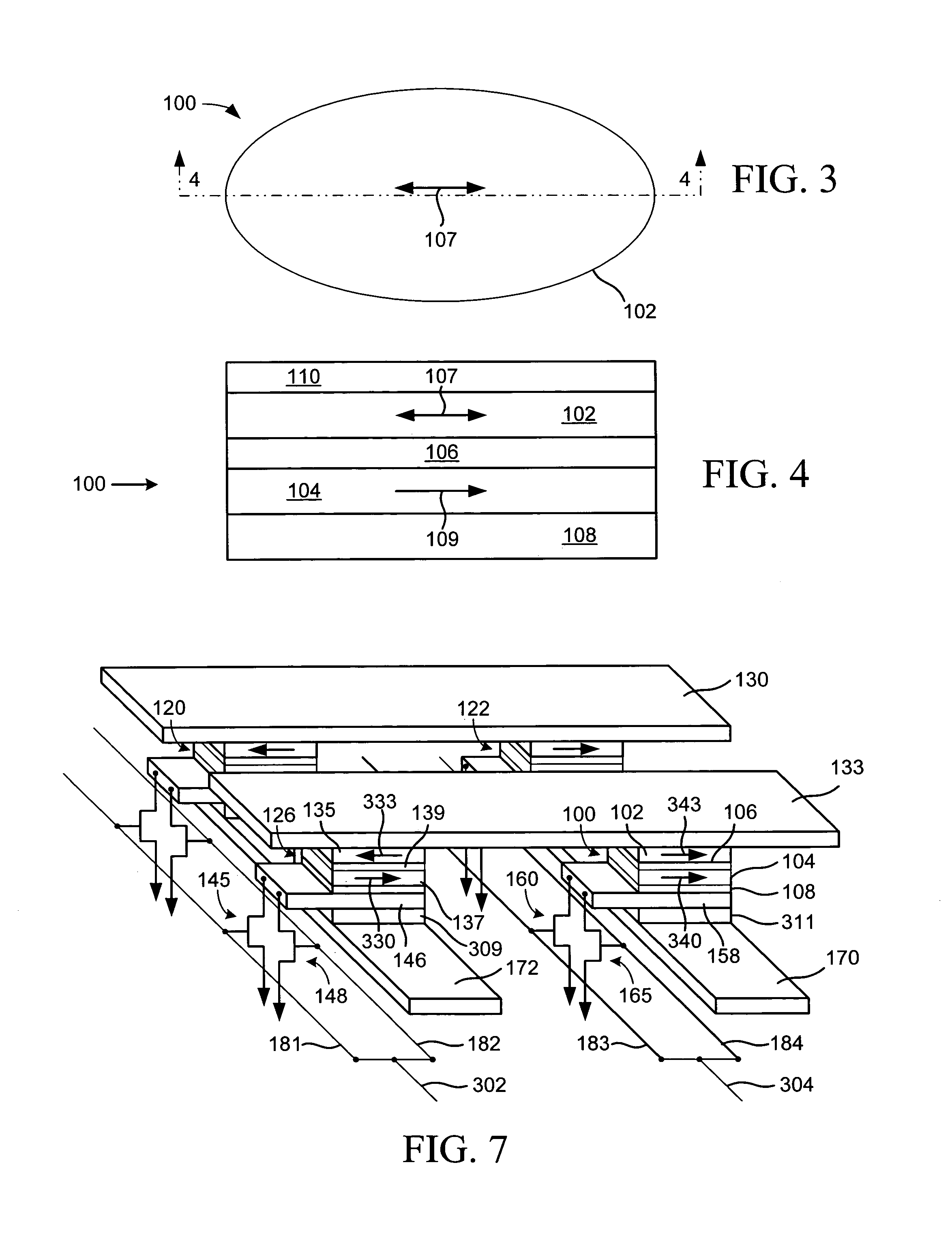
[0019]FIG. 3 is a top view and FIG. 4 is a cross-sectional view of a SDT device 100 including a tunnel barrier layer 106. The device includes a first FM layer 102 and second FM layer 104 separated by the tunnel barrier layer 106. A pinning structure 108 stabilizes a magnetic moment of the second FM layer 104. Other elements, such as an electrically conductive capping layer 110 may optionally be part of cell 100. In response to an applied magnetic field, the magnetic moment of the first FM layer 102 changes direction, as shown by arrow 107, while the magnetic moment of the second FM layer 104 is pinned, as shown by arrow 109. In this embodiment, which may for example be used in a MRAM device, an easy axis of magnetization of the first FM layer may be substantially parallel to the direction of magnetization of the second FM layer 104, so that the first FM layer switches between substantially parallel and substantially antiparallel states. As long as the easy axis of magnetization of t...


PUM


Abstract

A magnetic random access memory (MRAM) device has increased ΔR/R for sensing a state of a pin-dependent tunneling (SDT) device. The MRAM device includes plural transistors connected to a read line for sensing the state of the SDT device. Plural transistors lower an underlying resistance during reading, increasing ΔR/R. The plural transistors can share a source region.

Description

TECHNICAL FIELD[0001]This invention relates to solid state memory such as magnetic random access memory (MRAM) that may, for example, be employed in computers, consumer electronics and other digital processing systems.BACKGROUND[0002]Spin-dependent tunneling (SDT) effects are believed to depend upon a quantum mechanical probability of electron tunneling from one ferromagnetic (FM) electrode to another through a thin, electrically nonconductive layer, with the probability of tunneling depending upon the direction of magnetization of one electrode relative to the other. SDT effects have many potential applications in magnetic field sensing devices, such as magnetic field sensors and information storage and retrieval devices. Read transducers for magnetic heads used in disk or tape drives, which may be termed magnetoresistive (MR) sensors, and solid-state memory devices such as magnetic random access memory (MRAM), are potential commercial applications for spin tunneling effects.[0003]...

Claims


Application Information

Patent Timeline
IPC IPC(8): G11C11/00
CPCG11C11/16
Inventor SIN, KYUSIKGIBBONS, MATTHEW R.JENSEN, WILLIAM D.HINER, HUGH CRAIGSHI, XIZENG STONEBEZ, ROBERTOCASAGRANDE, GIULIOCAPPELLETTI, PAOLO
Owner MICRON TECH INC
Why Eureka
Try Eureka