Technique for forming the deep doped columns in superjunction

a superjunction and column technology, applied in the field of semiconductor devices, can solve the problems of difficult to avoid non-uniformities in the dopant gradient of columns, rapid increase in resistance of devices, and difficult to resist rapid increase in resistan

Inactive Publication Date: 2006-03-21
THIRD DIMENSION 3D SEMICON
View PDF41 Cites 43 Cited by
  • Summary
  • Abstract
  • Description
  • Claims
  • Application Information

AI Technical Summary

Problems solved by technology

Unfortunately, as curve 20 shows, the on-resistance of the device increases rapidly as its breakdown voltage increases.
This rapid increase in resistance presents a problem when the MOSFET is to be operated at higher voltages, particularly at voltages greater than a few hundred volts.
Unfortunately, non-uniformities in the dopant gradient of the columns can be difficult to avoid as a result of limitations in the control of process parameters during their fabrication.
Unfortunately, epitaxial deposition steps are expensive to perform and thus this structure is expensive to manufacture.
However, the on-resistance of a device that uses the floating island technique is not as low as an identical device that uses continuous columns.

Method used


Image

  • Technique for forming the deep doped columns in superjunction
  • Technique for forming the deep doped columns in superjunction
  • Technique for forming the deep doped columns in superjunction

Examples


Embodiment Construction

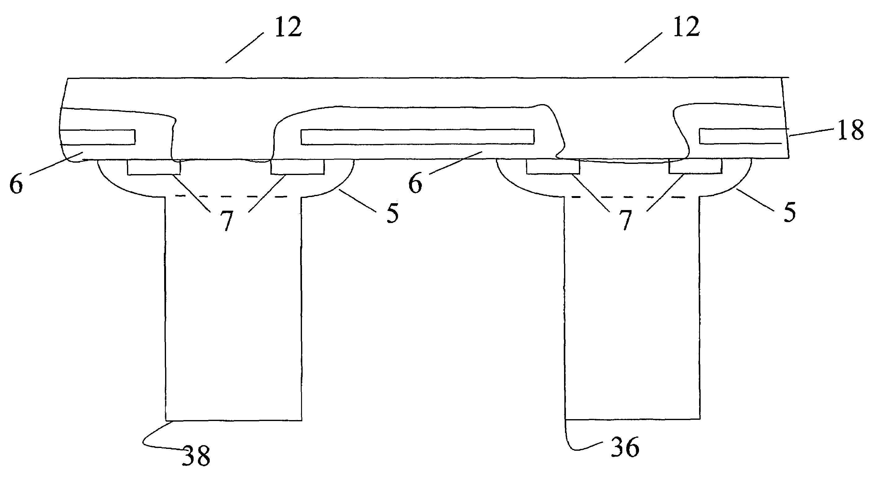
[0027]A technique for forming lightly doped columns that extend almost through a layer of deposited epitaxial semiconductor material is best understood by referring to FIGS. 4–18 while reading the description below. This technique uses trenches etched into the silicon to form lightly doped columns. One type of trenches has a dimension in a first direction that is greater than the dimension in a second direction that is perpendicular to the first direction and is generally rectangular shaped, while a second type is cross-shaped. FIG. 16 shows the top view of a series of generally rectangular shaped trenches 35 following two separate implantation steps that have doped the two narrow walls 31 and 33 of the trenches 35. FIGS. 9 and 10 show the technique that is used to perform the two implantation steps. The two separate implantation steps are performed at an angle with respect to the surface of the substrate that allows the dopant to be implanted into just the two narrow “end” sidewall...


PUM


Abstract

A method of manufacturing a semiconductor device is disclosed and starts with a semiconductor substrate having a heavily doped N region of at the bottom main surface and having a lightly doped N region at the top main surface. There are a plurality of trenches in the substrate, with each trench having a first extending portion extending from said top main surface towards the heavily doped region. Each trench has two sidewall surfaces in parallel alignment with each other. A blocking layer is formed on the sidewalls and the bottom of each trench. Then a P type dopant is obliquely implanting into the sidewall surfaces to form P type doped regions. The blocking layer is then removed. The bottom of the trenches is then etched to remove any implanted P type dopants. The implants are diffused and the trenches are filled.

Description

[0001]This application claims the benefit of Provisional Application No. 60 / 474,127, filed May 29, 2003.FIELD OF THE INVENTION[0002]The present invention relates generally to semiconductor devices, and more, particularly, to power MOSFET devices.BACKGROUND OF THE INVENTION[0003]Power MOSFET devices are employed in applications such as automobile electrical systems, power supplies, and power management applications. Such devices should sustain high voltage in the off-state while having a low voltage drop and high current flow in the on-state.[0004]FIG. 1 illustrates a typical structure for an N-channel power MOSFET. An N-epitaxial silicon layer 1 formed over an N+ silicon substrate 2 contains p-body regions 5a and 6a, and N+ source regions 7 and 8 for two MOSFET cells in the device. P-body regions 5 and 6 may also include deep p-body regions 5b and 6b. A source-body electrode 12 extends across certain surface portions of epitaxial layer 1 to contact the source and body regions. The N...

Claims


Application Information

Patent Timeline
Patent Type & Authority Patents(United States)
IPC IPC(8): H01L21/336
CPCH01L21/26586H01L29/0634H01L27/088H01L29/66712H01L29/7802H01L29/7811H01L29/0653H01L29/0696H01L29/1095
Inventor BLANCHARD, RICHARD A.
Owner THIRD DIMENSION 3D SEMICON
Why Eureka
Try Eureka