Method and system for electrically coupling a chip to chip package

a technology of electrical coupling and semiconductor chips, applied in the direction of semiconductor devices, semiconductor/solid-state device details, electrical apparatus, etc., can solve the problems of increasing electrical resistance in connection and compromising the electrical connection of the chip to the chip packag

Inactive Publication Date: 2006-03-21
MICRON TECH INC
View PDF13 Cites 17 Cited by
  • Summary
  • Abstract
  • Description
  • Claims
  • Application Information

AI Technical Summary

Problems solved by technology

Each wire 6 must be placed individually, which is time consuming, and each wire results in increased electrical resistance in the connection.
Additionally, given the orientation of the chip 2 and the chip package 4, after bonding an efficient visual inspection of the bonds is not possible, and the nature of the bonding procedure mandates that the chip 2 be heated and exposed to pressure.
Even slight misalignment can result in multiple short circuits and missed connections between inner leads and chip pads, thus compromising the electrical connection of the chip to the chip package.

Method used


Image

  • Method and system for electrically coupling a chip to chip package
  • Method and system for electrically coupling a chip to chip package
  • Method and system for electrically coupling a chip to chip package

Examples


Embodiment Construction

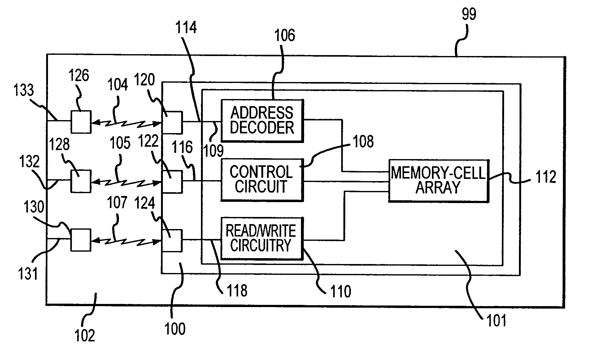
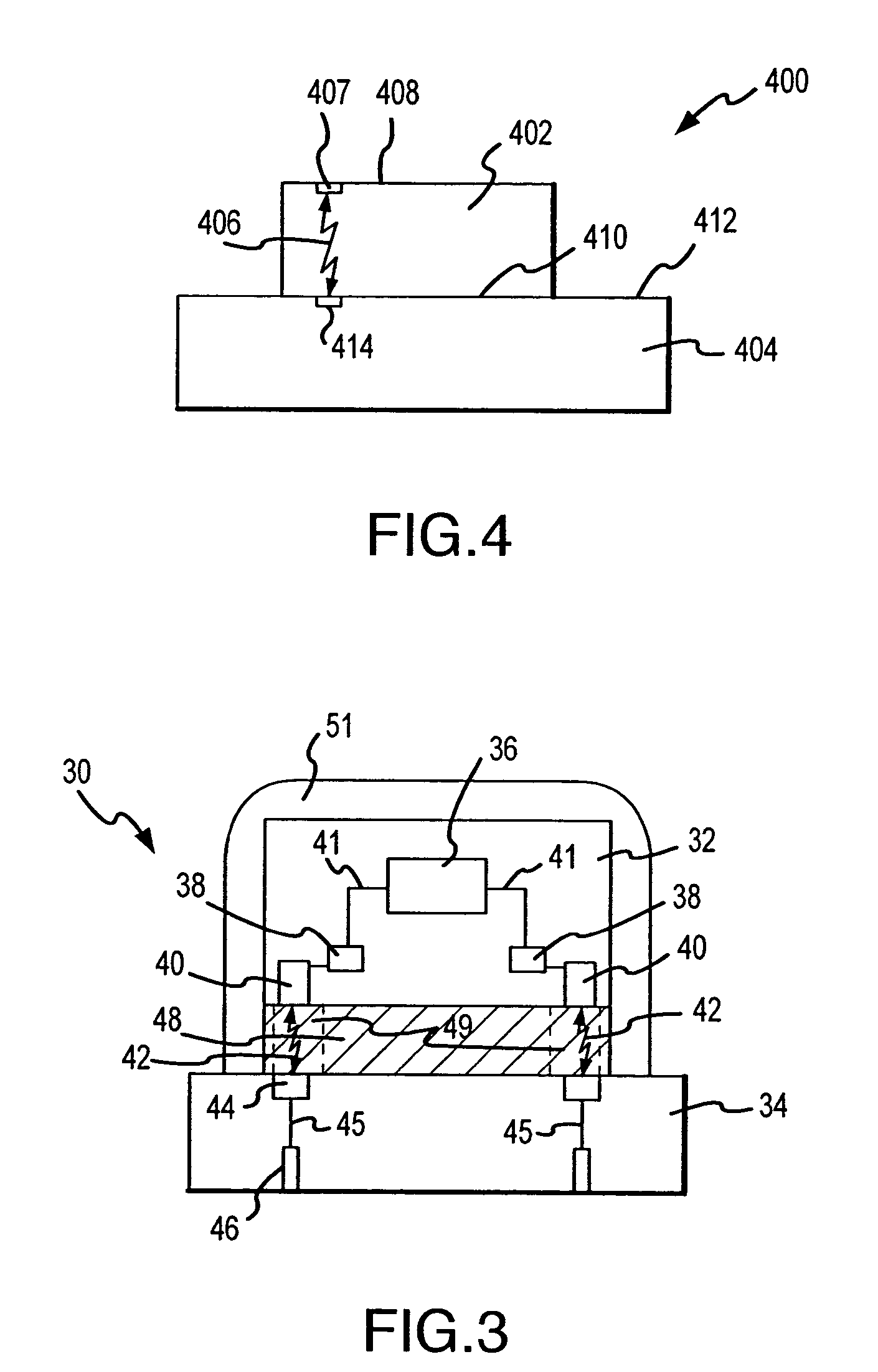
[0016]FIG. 3 is a functional and cross-sectional view of a microelectronics package 30 including a chip 32 that is coupled to a chip package 34 through electromagnetic signals 42, as will now be explained in more detail. By coupling the chip 32 to the chip package 34 through electromagnetic signals 42, a direct physical connection between the two is eliminated, which can simplify the fabrication of the package 30 and reduce the adverse inductive and capacitive effects associated with conventional bonding techniques. The chip 32 includes electronic circuitry 36 coupled to bonding pads 38 which, in turn, are coupled to first converters 40. It is also possible for the circuitry 36 to be directly coupled to the converters 40 without the use of intervening bonding pads 38. The circuitry 36 in the chip 32 may be a memory device, a processor, or any other type of integrated circuitry.

[0017]Each first converter 40 receives a corresponding electric signal 41 from the circuitry 36 via the bon...


PUM


Abstract

A chip and a chip package can transmit information to each other by using a set of converters capable of communicating with each other through the emission and reception of electromagnetic signals. Both the chip and the chip package have at least one such converter physically disposed on them. Each converter is able to (1) convert received electromagnetic signals into electronic signals, which it then may relay to leads on the device on which it is disposed; and (2) receive electronic signals from leads on the device on which it is disposed and convert them into corresponding electromagnetic signals, which it may transmit to a corresponding converter on the other device. Not having a direct physical connection between the chip and the chip package decreases the inductive and capacitive effects commonly experienced with physical bonds.

Description

CROSS-REFERENCE TO RELATED APPLICATION[0001]This application is a Divisional of pending U.S. patent application Ser. No. 09 / 978,983, filed, Oct. 15, 2001.TECHNICAL FIELD[0002]The present invention is related generally to semiconductor integrated circuits, and more specifically to a method and system for electrically coupling a semiconductor chip to a chip package.BACKGROUND OF THE INVENTION[0003]During the manufacture of integrated circuit devices, such as memories and microprocessors, a semiconductor die or chip must be physically and electrically attached to a chip package. A chip is a small piece of semiconductor material, such as silicon, in which an integrated circuit is formed, and a chip package as used herein is a protective container, such as a plastic dual-in-line package (DIP), or printed circuit board to which the chip is coupled, as will be appreciated by those skilled in the art.[0004]To electrically couple a chip to a chip package, electrical connections are formed be...

Claims


Application Information

Patent Timeline
Patent Type & Authority Patents(United States)
IPC IPC(8): H01L31/0203H01L23/48
CPCH01L23/48H01L2924/0002H01L2924/00
Inventor MURPHY, TIMGOTCHER, LEE
Owner MICRON TECH INC
Why Eureka
Try Eureka