Two-dimensional semiconductor negative capacitance field-effect transistor and preparation method thereof

A two-dimensional semiconductor and capacitive field technology, which is applied in semiconductor/solid-state device manufacturing, semiconductor devices, circuits, etc., can solve the problem of inability to break through the sub-threshold swing of devices, mutual constraints of power consumption-performance-scale, and high-integration power consumption Unable to solve other problems, achieve the effect of reducing the sub-threshold swing, simple structure, and high switching ratio

Pending Publication Date: 2017-09-22
SHANGHAI INST OF TECHNICAL PHYSICS - CHINESE ACAD OF SCI
View PDF4 Cites 17 Cited by
  • Summary
  • Abstract
  • Description
  • Claims
  • Application Information

AI Technical Summary

Problems solved by technology

Although this type of device has achieved a small scale, the power consumption caused by high integration still cannot be solved, and the sub-threshold swing of the device still cannot exceed 60mV / dec, and it also faces the problem of mutual constraints of power consumption-performance-scale

Method used


Image

  • Two-dimensional semiconductor negative capacitance field-effect transistor and preparation method thereof
  • Two-dimensional semiconductor negative capacitance field-effect transistor and preparation method thereof
  • Two-dimensional semiconductor negative capacitance field-effect transistor and preparation method thereof

Examples


example 1

[0041] Example 1 of the present invention is described in detail below in conjunction with accompanying drawing:

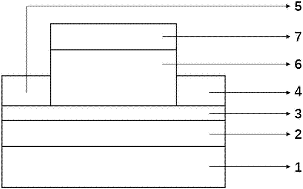
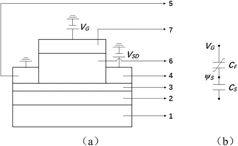
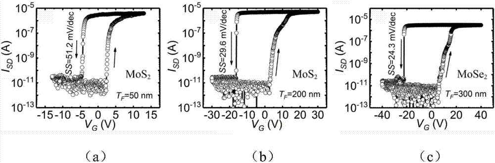
[0042] The invention develops a two-dimensional semiconductor negative capacitance field effect transistor. Utilize the negative capacitance effect of P(VDF-TrFE) ferroelectric polymer material to amplify the externally applied gate voltage, strengthen the control of the carrier and energy band of the two-dimensional semiconductor material, so as to effectively reduce the sub-scale of the field effect transistor device. Threshold swing, increase the device turnover rate, reduce the overall power consumption of the device.

[0043] Specific steps are as follows:

[0044] 1. Substrate selection

[0045] A heavily doped p-type silicon with a thickness of 0.5 mm is selected as the substrate.

[0046] 2. Preparation of oxide dielectric layer

[0047] The silicon dioxide with a thickness of 285±5 nanometers is oxidized on the surface of the silicon substrate by a th...

example 2

[0059] Example 2 of the present invention is described in detail below in conjunction with accompanying drawing:

[0060] The invention develops a two-dimensional semiconductor negative capacitance field effect transistor. Utilize the negative capacitance effect of P(VDF-TrFE) ferroelectric polymer material to amplify the externally applied gate voltage, strengthen the control of the carrier and energy band of the two-dimensional semiconductor material, so as to effectively reduce the sub-scale of the field effect transistor device. Threshold swing, increase the device turnover rate, reduce the overall power consumption of the device.

[0061] Specific steps are as follows:

[0062] 5. Substrate selection

[0063] A heavily doped p-type silicon with a thickness of 0.5 mm is selected as the substrate.

[0064] 6. Preparation of oxide dielectric layer

[0065] The silicon dioxide with a thickness of 285±5 nanometers is oxidized on the surface of the silicon substrate by a th...

example 3

[0077] Example 3 of the present invention is described in detail below in conjunction with accompanying drawing:

[0078] The invention develops a two-dimensional semiconductor negative capacitance field effect transistor. Utilize the negative capacitance effect of P(VDF-TrFE) ferroelectric polymer material to amplify the externally applied gate voltage, strengthen the control of the carrier and energy band of the two-dimensional semiconductor material, so as to effectively reduce the sub-scale of the field effect transistor device. Threshold swing, increase the device turnover rate, reduce the overall power consumption of the device.

[0079] Specific steps are as follows:

[0080] 1. Substrate selection

[0081] A heavily doped p-type silicon with a thickness of 0.5 mm is selected as the substrate.

[0082] 2. Preparation of oxide dielectric layer

[0083] The silicon dioxide with a thickness of 285±5 nanometers is oxidized on the surface of the silicon substrate by a th...


PUM


Abstract

The invention discloses a two-dimensional semiconductor negative capacitance field-effect transistor and a preparation method thereof. The device structure sequentially comprises a substrate, a two-dimensional semiconductor, a metal source-drain electrode, a ferroelectric gate medium with a negative capacitance effect and a metal gate electrode from bottom to top. The preparation method comprises the steps of firstly, preparing the transition metal chalcogenide two-dimensional conductor on a substrate; secondly, preparing the metal source-drain electrode by employing an electron beam lithography technology and combining a stripping process; thirdly, preparing a ferroelectric thin film with the negative capacitance effect on the structure; and finally, preparing the metal gate electrode on the thin film to form ferroelectric-controlled two-dimensional semiconductor negative capacitance field-effect transistor. Different from other two-dimensional semiconductor negative capacitance field-effect device structures, the metal-ferroelectric-semiconductor structure has the advantages that a high-performance negative capacitance field-effect device can be achieved; and an electrical test result shows that the subthreshold swing of the device is far smaller than 60mV / dec, the Boltzmann limit is broken through, and the two-dimensional semiconductor negative capacitance field-effect device simultaneously has the characteristics of extremely low power consumption, high-speed turnover and the like.

Description

technical field [0001] The invention relates to a low-power low-dimensional semiconductor electronic device, in particular to a two-dimensional semiconductor material negative capacitance field-effect transistor regulated and controlled based on a ferroelectric material and a preparation method thereof. Background technique [0002] With the development of integrated circuit technology, this technology has been widely used in various electronic products. Due to the continuous improvement of integration, while the performance of electronic products is improved, reducing power consumption is also an inevitable trend in the development of electronic products. Under the traction of Moore's Law, the size of traditional field effect transistor devices has been continuously reduced and the integration level has been continuously improved, resulting in an increase in chip power consumption. However, because the traditional field effect transistor is based on the hot carrier diffusio...

Claims


Application Information

Patent Timeline
Patent Type & Authority Applications(China)
IPC IPC(8): H01L29/78H01L29/51H01L21/34H01L21/445
CPCH01L29/516H01L29/66969H01L29/78H01L21/445
Inventor 王建禄王旭东孟祥建沈宏林铁孙硕孙璟兰褚君浩
Owner SHANGHAI INST OF TECHNICAL PHYSICS - CHINESE ACAD OF SCI
Why Eureka
Try Eureka