System and method for serial ion implanting productivity enhancements

a technology of serial ion and productivity enhancement, applied in the field of system and method for serial ion implanting productivity enhancement, can solve the problems reduce the potential system throughput, and achieve the effects of poor utilization of ion beam on wafer, reduced potential system throughput, and low utilization of ion beam

Active Publication Date: 2006-03-28
VARIAN SEMICON EQUIP ASSOC INC
View PDF1 Cites 2 Cited by
  • Summary
  • Abstract
  • Description
  • Claims
  • Application Information

AI Technical Summary

Benefits of technology

[0006]In serial implant ion implanters, the ion beam utilization is low. This is due to the presence of a wafer holding device, or platen, for processing (ion implanting) and wafer exchange. The time to exchange a processed wafer to an unprocessed wafer is in series with the implant process. The utilization of the ion beam on wafer is poor due to wafer exchange occurring in the critical path of the implantation process. This reduces the potential system throughput due to ion beam non-utilization during wafer exchange. The present invention is directed to utilizing a plurality of single wafer holding devices to approach continuous implantation relative to the beam, thus enabling wafer exchange to occur in parallel with the implantation process. As a result, significant system productivity improvement and wafer throughput will be realized.

Problems solved by technology

The utilization of the ion beam on wafer is poor due to wafer exchange occurring in the critical path of the implantation process.
This reduces the potential system throughput due to ion beam non-utilization during wafer exchange.

Method used


Image

  • System and method for serial ion implanting productivity enhancements
  • System and method for serial ion implanting productivity enhancements
  • System and method for serial ion implanting productivity enhancements

Examples


Embodiment Construction

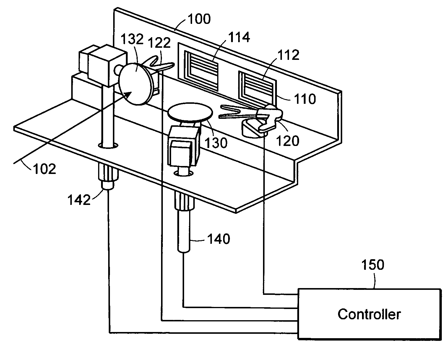
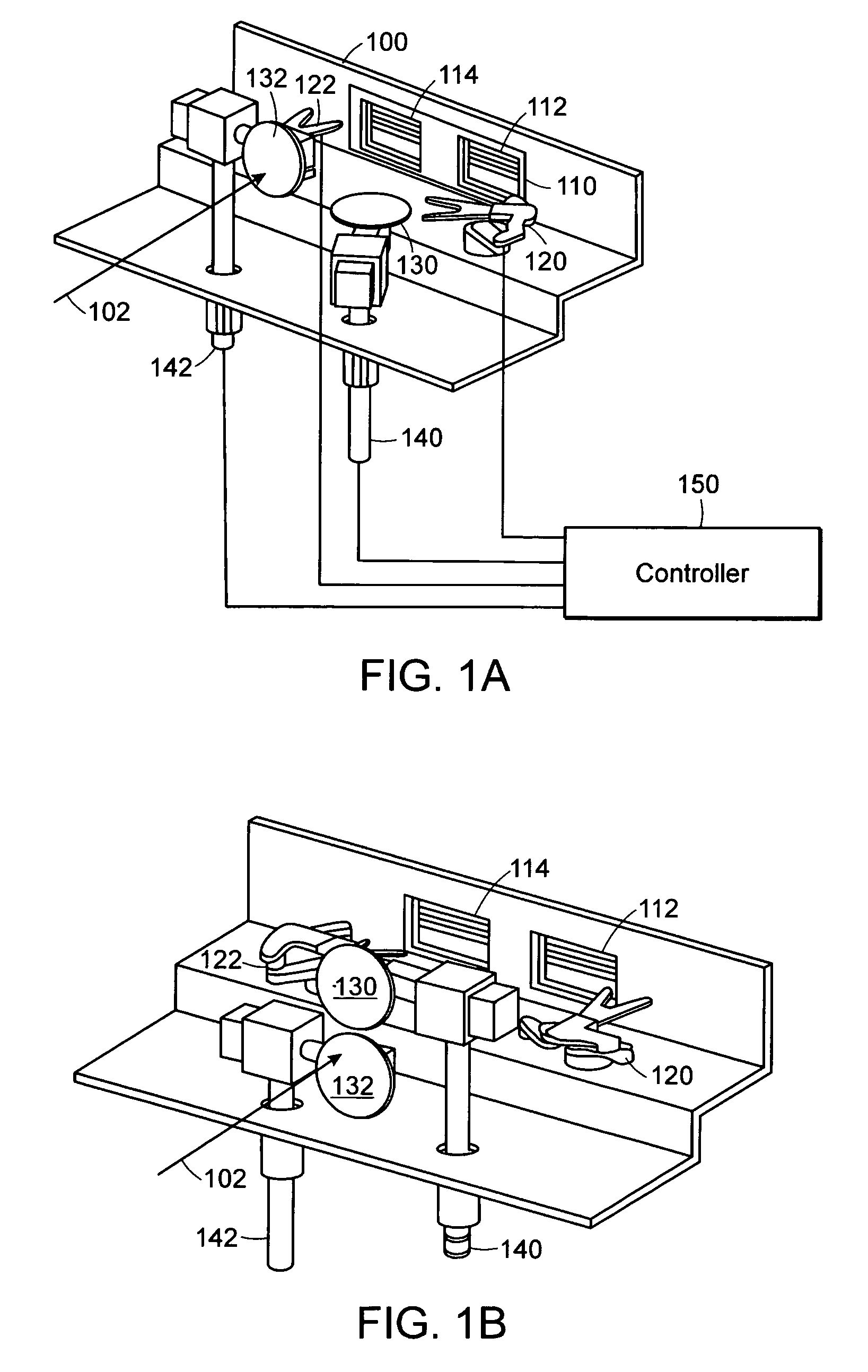
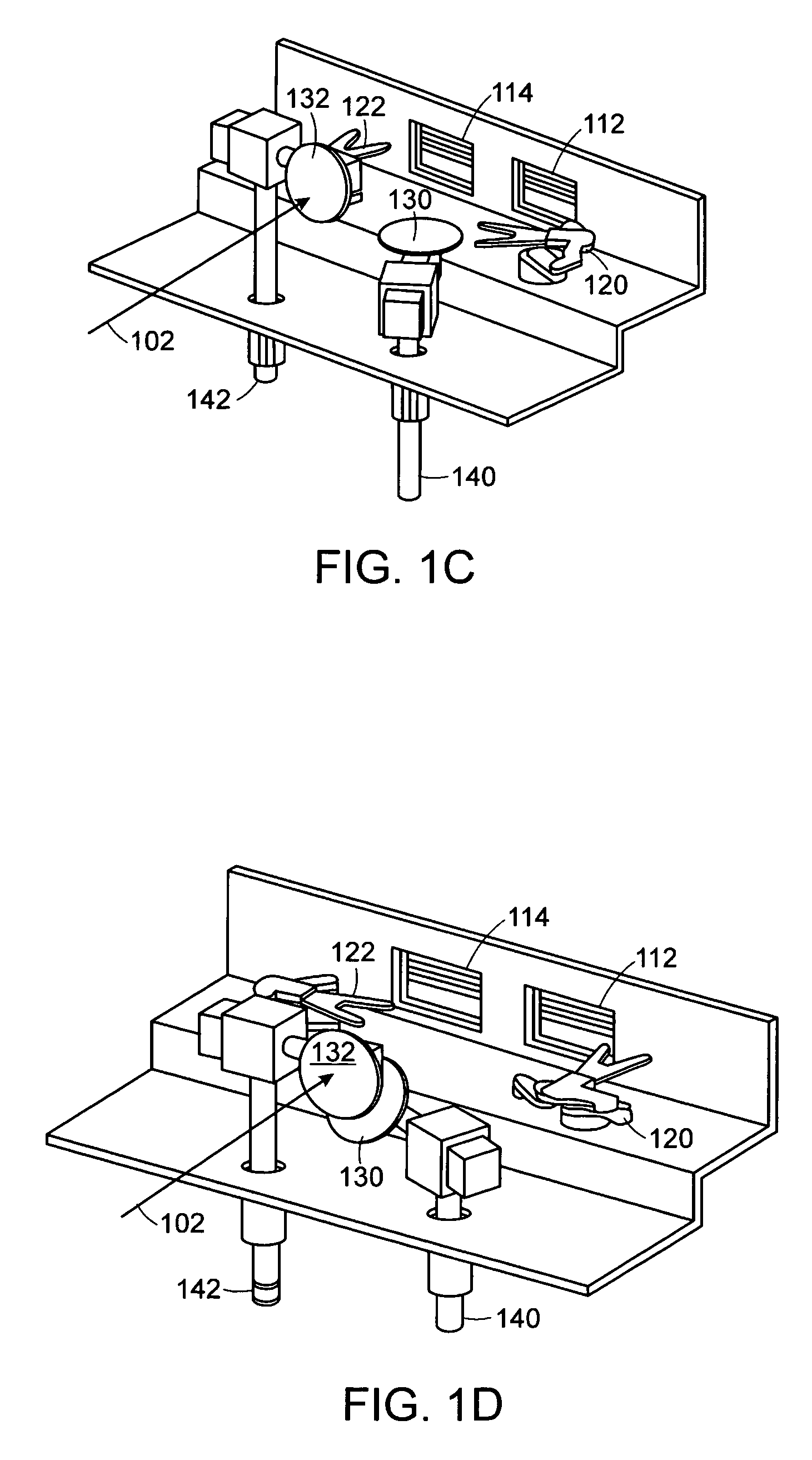
[0011]According to the present invention, a system is provided for a high efficiency utilization of an ion beam while implanting semiconductor wafers. FIGS. 1(a)–1(g) illustrate examples of a system 100 for a two platen serial ion implanter according to an embodiment of the present invention. The system includes a load lock 110 for holding pass through cassettes of workpieces or wafers, which are passed from atmosphere (load area) to a vacuum area (implanting area) and then back after the ion implanting process is completed. First and second workpiece exchangers 120 and 122 are positioned between the load lock 110 and the first and second platens 130 and 132 for moving workpieces therebetween. The first and second workpiece exchangers 120 and 122 may be dual arm, multi-link or scara robots or the equivalent workpiece / wafer moving devices. In the present embodiment, the load lock 110 includes two load lock chambers 112 and 114 which are associated with the first and second platens 13...


PUM


Abstract

An ion implantation apparatus is provided for workpiece handling. The apparatus includes a plurality of scan systems for scanning workpieces in an ion implanting beam, a plurality of exchangers for moving the workpieces to and from the scan systems, and a system controller for positioning one of the workpieces for scanning in the ion implanting beam by one of the scan systems, sensing completion of the ion beam scanning for the one workpiece and simultaneously positioning another of the workpieces for scanning in the ion implanting beam by another of the scan systems so that the workpieces are continuously presented to the ion implanting beam. The apparatus provides continuous implantation relative to the beam, thus enabling wafer exchange to occur in parallel with the implantation process. As a result, significant system productivity improvement and wafer throughput will be realized.

Description

RELATED APPLICATIONS[0001]This application claims priority under 35 U.S.C. § 119(e) to U.S. Provisional Patent Application Ser. No. 60 / 527,977, filed Dec. 8, 2003, entitled “System and Method for Serial Ion Implanting Productivity Enhancements,” the disclosure of which is hereby incorporated by reference.FIELD OF THE INVENTION[0002]The described system and method relate generally to maximizing the beam on wafer time during serial ion implantation processing. More particularly, the described system and method are directed to maximizing the presence of a wafer in front of the beam path so that the utilization of the beam for implanting is maximized.BACKGROUND OF THE INVENTION[0003]The processing of semiconductor wafers involves processing tools for performing a large number of processing steps. The processing steps are usually performed in a vacuum chamber. The processing tools typically handle and process wafers one at a time in order to optimize control and reproducibility. These pr...

Claims


Application Information

Patent Timeline
Patent Type & Authority Patents(United States)
IPC IPC(8): H01J37/08H01J37/00H01J37/147H01J37/317
CPCH01J37/3171H01J37/1474
Inventor SHENG, ALAN P.RIORDON, BENJAMIN B.FICARRA, LAWRENCE M.
Owner VARIAN SEMICON EQUIP ASSOC INC
Why Eureka
Try Eureka