Unlock instant, AI-driven research and patent intelligence for your innovation.

Method and apparatus for dynamically hiding a defect in an embedded memory

a defect and memory technology, applied in the field of memory, can solve the problems of unrecoverable loss, inability to dynamically hide a defect in the memory, and inevitably certain percentage of memory with memory defects, and achieve the effect of reducing the memory volum

Inactive Publication Date: 2006-03-28
MACRONIX INT CO LTD
View PDF8 Cites 6 Cited by
  • Summary
  • Abstract
  • Description
  • Claims
  • Application Information

AI Technical Summary

Benefits of technology

The present invention proposes a method and apparatus to mask memory defects instead of repairing them by blowing fuses. This avoids lengthy procedures of testing, repairing and retesting. The invention may also reduce memory volume, allow for the use of defective chips, and avoid disposing of them. The method dynamically excludes memory defects by discovering and hiding them each time the chip with the defects is powered up. It also avoids large and redundant circuitry introduced into the memory chip for excluding memory defects, avoids recalculating memory size and addresses resulting from the memory defects, and preserves the functional circuit on a chip with embedded memory. The invention provides an initial test to discover defective entries, an entry occupied mapping that contains a plurality of fields where each filed corresponds to an entry of the memory, and an initialization control apparatus to mark the fields corresponding to defective entries to make them be perceived as occupied so that the defective entries will not be accessed until the system is shut down. A backup memory or backup register pool is provided and an error entry recorder / controller is used to record error entries and pick up a pseudo entry from the backup memory or backup register pool for corresponding to each respective error entry after the memory goes through an initial test. A subsequent access to an error entry results in a redirect to the corresponding pseudo entry.

Problems solved by technology

Memory defects can result in malfunction of a system utilizing the defective memory and cause an abrupt shutdown without warning in advance, which not only takes the user considerable time, but also may cause unrecoverable loss.
Unfortunately, there is a inevitably certain percentage of memory with memory defects.
However, disposing of defective memory leads to economic loss, and it is especially regrettable to discard a chip because of minor defects.
Even though repairing memory by using a redundancy scheme can reduce memory waste, the additional circuitry and fuses consume considerable chip area and complicate the circuit as well as the process.
This not only increases the cost but also enlarges the chip.
Furthermore, such repairing requires a lot of time on testing and analyzing, which further increases the time and cost.
The problem due to memory defects is more severe for a chip with embedded memory because its circuitry is much more complicated than that of a stand-alone memory chip.
A chip with embedded memory has a lot of circuitry around the memory, and it is thus more difficult to test the memory, and the tester is also more expensive and the test procedure is longer.
As the demand for larger embedded memory grows, the yield limitation imposed by the manufacturing process is also enlarged.
Although a redundancy test is typically used as a functional test, this method often proves itself not enough or not applicable for larger embedded memory.
However, the above-mentioned prior art schemes can only filter out the defects found upon testing and fixed by repair, and any defects discovered or developed thereafter cannot be remedied and eventually the chip with memory defects in such manner must still be discarded.
More seriously is that defects occurring in a memory after the test procedure will cause the chip to malfunction or a system to crash, thereby resulting in even larger loss.
These inconveniences render this technique impractical and the system will crash once there are too many defects, exceeding what the redundant circuit can repair.
However, it is inconvenient to recalculate the effective memory size and modify the memory addresses, and the extra circuitry to modify the memory address occupies considerable chip area.
Furthermore, due to the fact that its memory address space is continuous, remapping the memory address cannot exclude a single memory defect, but instead starts from the next available entry following the defective entry, and thus the entries before the defective memory are wasted.

Method used


Image

  • Method and apparatus for dynamically hiding a defect in an embedded memory
  • Method and apparatus for dynamically hiding a defect in an embedded memory
  • Method and apparatus for dynamically hiding a defect in an embedded memory

Examples


Embodiment Construction

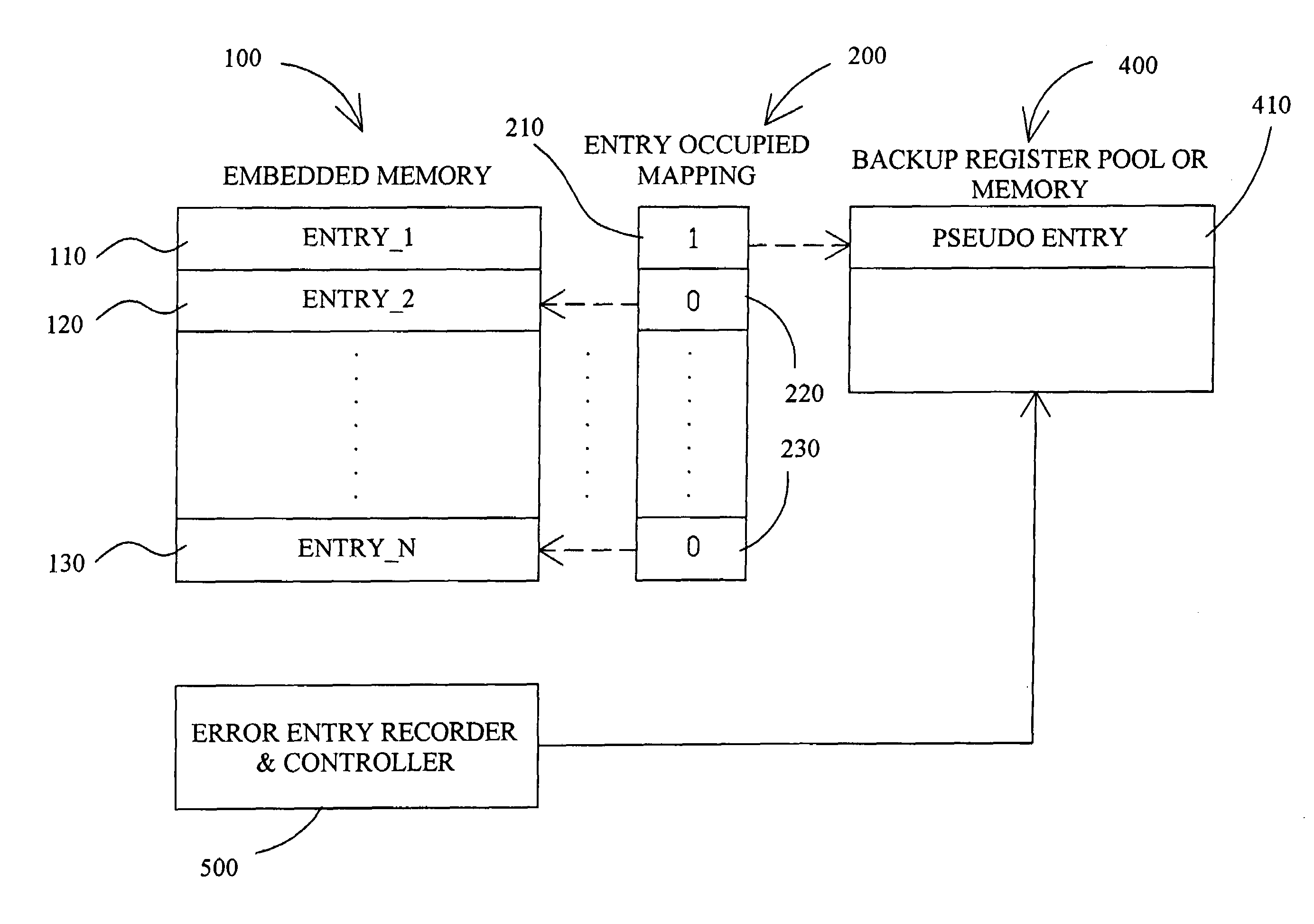
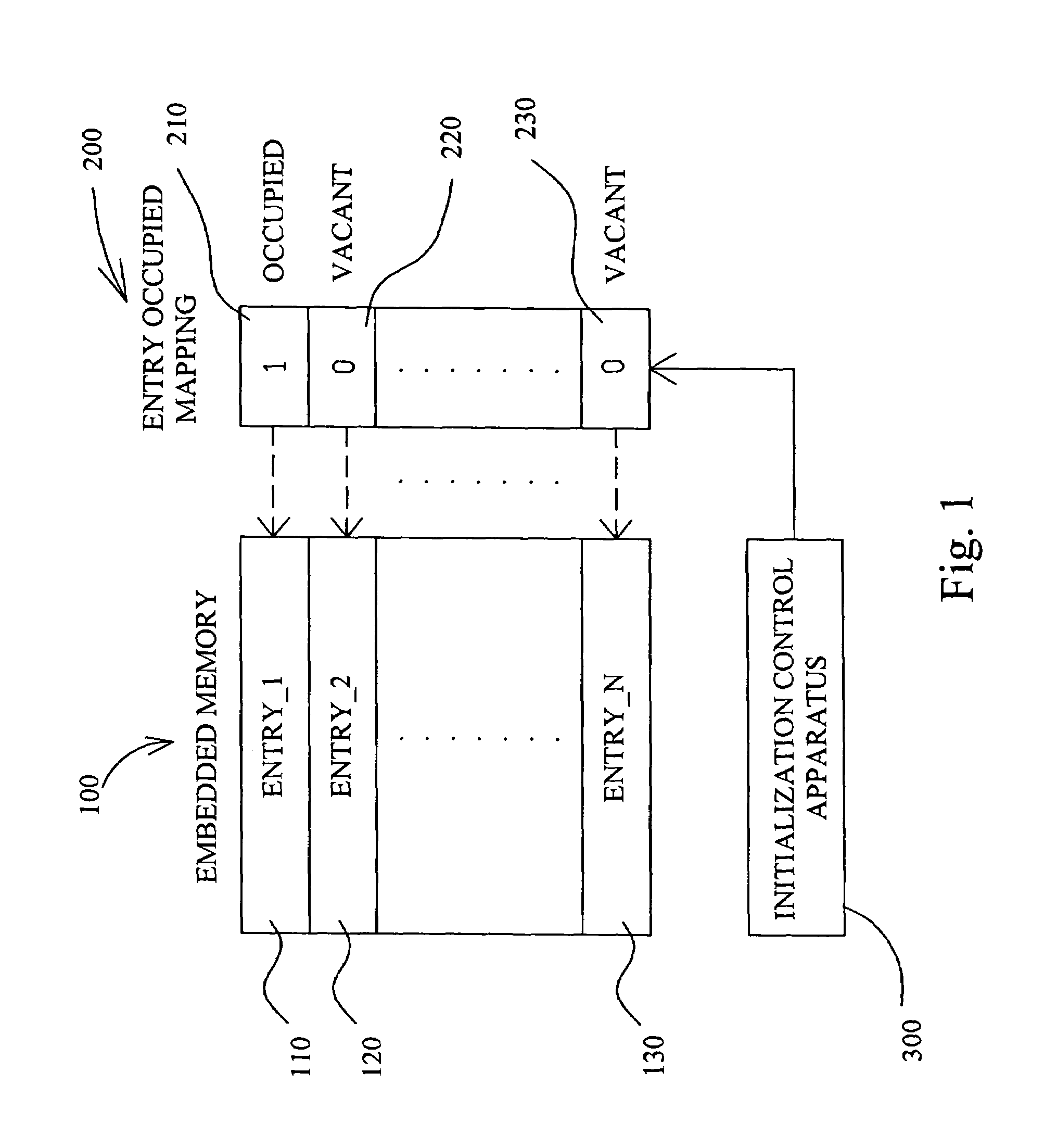
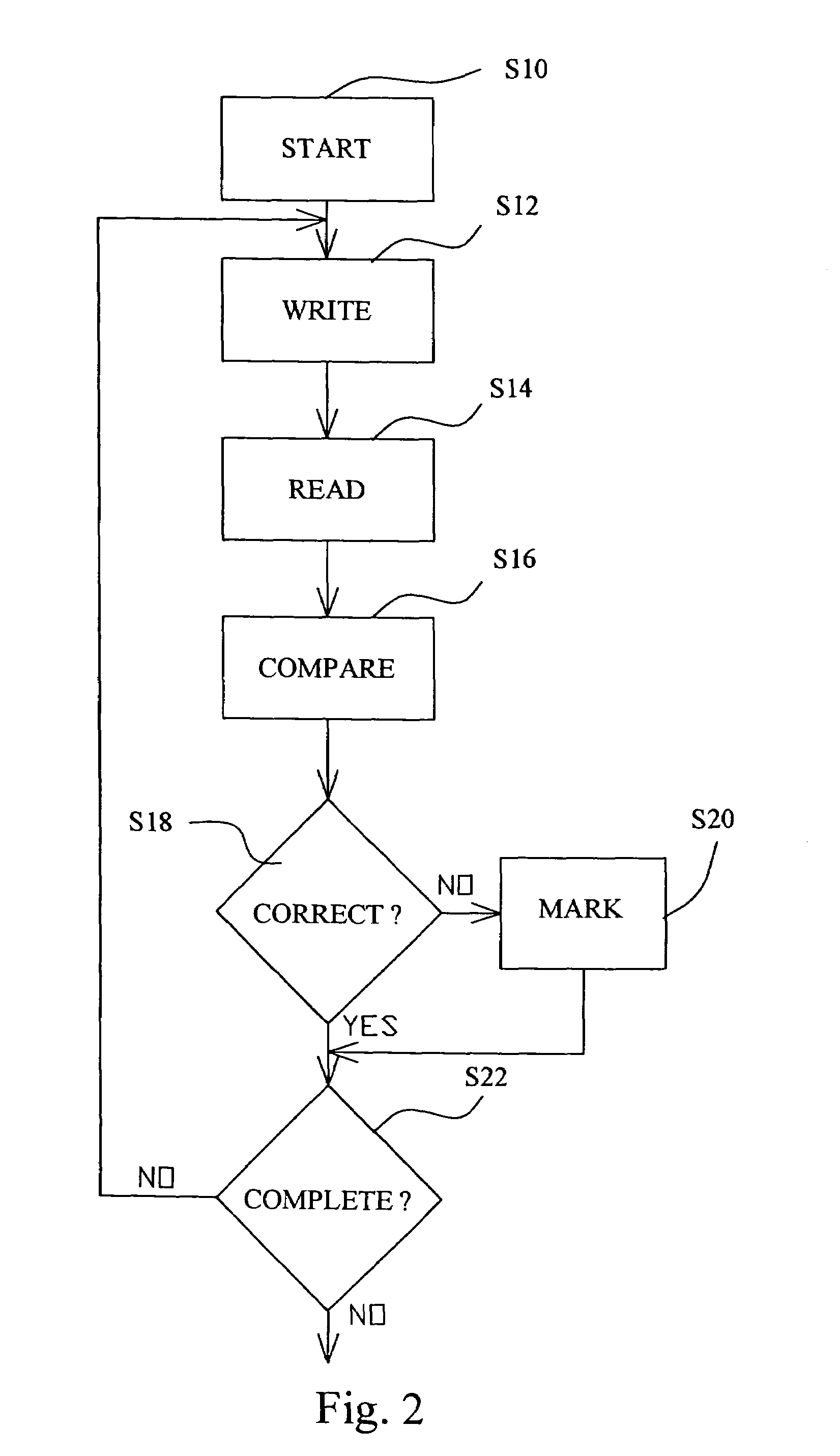
[0023]A method and apparatus are disclosed to handle defects in a memory, especially in a memory embedded in a chip, from a different point of view, by which the memory defects are hidden so that it looks as it used to be, instead of repairing the memory by fuses or dealing with the memory size, and thereby the user does not know that the memory is defective. The method detects the locations of defective entries by the test procedure already scheduled during a system boot-up, without introducing an additional test procedure as well as repair and retest procedures, and thus it is not necessary to spend lengthy processing time. Furthermore, only simple apparatus is used for marking or recording memory defects, so there is thus no need to include a complex processing circuit. Though it results in memory size reduction in this manner, the invented method and apparatus also make a chip with a defective memory usable instead of needing to be discarded. The invented technique dynamically e...


PUM


Abstract

A method and apparatus are provided for dynamically hiding a defect in a memory. In one embodiment, an entry occupied mapping includes a plurality of fields each corresponding to an entry of a memory, and during the initial test procedure of the memory the field corresponding to a defective entry is marked to make it perceived as occupied and thus the defective entry will not be used hereafter. In another embodiment, pseudo entries are selected from a backup register pool or backup memory. Each pseudo entry corresponds to a defective entry, and subsequent access to the defective entry is redirected to the corresponded pseudo entry.

Description

CROSS-REFERENCE TO RELATED APPLICATION[0001]This application is a divisional of application Ser. No. 10 / 212,079, which was filed on Aug. 6, 2002 (now U.S. Pat. No. 6,836,438, issued on Dec. 28, 2004).FIELD OF THE INVENTION[0002]The present invention relates generally to a memory and, more specifically, to a method and apparatus for dynamically hiding a defect in a memory. The invented method and apparatus is particularly useful and suitable for a chip with an embedded memory.BACKGROUND OF THE INVENTION[0003]Memory defects can result in malfunction of a system utilizing the defective memory and cause an abrupt shutdown without warning in advance, which not only takes the user considerable time, but also may cause unrecoverable loss. Unfortunately, there is a inevitably certain percentage of memory with memory defects. Usually a test is performed immediately after the manufacture of the chip, so that defective memory can be found and disposed of. However, disposing of defective memory...

Claims


Application Information

Patent Timeline
Patent Type & Authority Patents(United States)
IPC IPC(8): G11C7/00G11C29/00G11C29/44
CPCG11C29/44G11C29/88G11C2207/104G11C2029/1208
Inventor CHEN, APHRODITE
Owner MACRONIX INT CO LTD
Features
  • R&D
  • Intellectual Property
  • Life Sciences
  • Materials
  • Tech Scout
  • Unparalleled Data Quality
  • Higher Quality Content
  • 60% Fewer Hallucinations
Learn More