Method and apparatus for determining chemistry of part's residual contamination

a residual contamination and chemistry technology, applied in semiconductor/solid-state device testing/measurement, data acquisition and logging, instruments, etc., can solve the problems of unusable metal contamination of semiconductor wafers being etched, parts are frequently exposed to toxic and dangerous chemistries, and cover can etch or otherwise become unusabl

Inactive Publication Date: 2006-03-28
TOKYO ELECTRON LTD
View PDF8 Cites 5 Cited by
  • Summary
  • Abstract
  • Description
  • Claims
  • Application Information

AI Technical Summary

Benefits of technology

[0010]Still a further object of the present invention is to provide the monitoring device with a capability to record the chemical history (i.e. the processing history) that the consumable part is exposed to.

Problems solved by technology

In the current semiconductor industry practice, many parts of semiconductor processing apparatus are treated as consumable parts either due to wear on the parts or due to the build up of excessively large film deposits which can contribute to particulate contamination of a semiconductor wafer process.
The free-standing window insert over time is replaced once its optical properties become insufficient for diagnostic purposes.
Such exposure can lead to undesirable metal contamination of the semiconductor wafer being etched.
Over time, the cover can etch or otherwise become unusable requiring that it be replaced.
Accordingly, one important environmental, health, and safety (EHS) issue in the semiconductor industry becomes that of disposal of used consumable parts from semiconductor processing tools.
These parts are frequently exposed to toxic and dangerous chemistries during the lifetime of the consumable parts on the tool.
In an environment where different wafer batches are subjected to different processes on the same tool, such as in a foundry semiconductor manufacturing plant, it is difficult to track what chemistries have been used in the tool since the consumable part was last replaced.
Furthermore, it is typical that when maintenance on the tool is performed, there is no knowledge of the chemistries that the consumable parts have been exposed to, leading in some cases to the use of the safest, and invariably most expensive disposal approach.
Such a fail-safe approach raises the cost of semiconductor processing.

Method used


Image

  • Method and apparatus for determining chemistry of part's residual contamination
  • Method and apparatus for determining chemistry of part's residual contamination
  • Method and apparatus for determining chemistry of part's residual contamination

Examples


Embodiment Construction

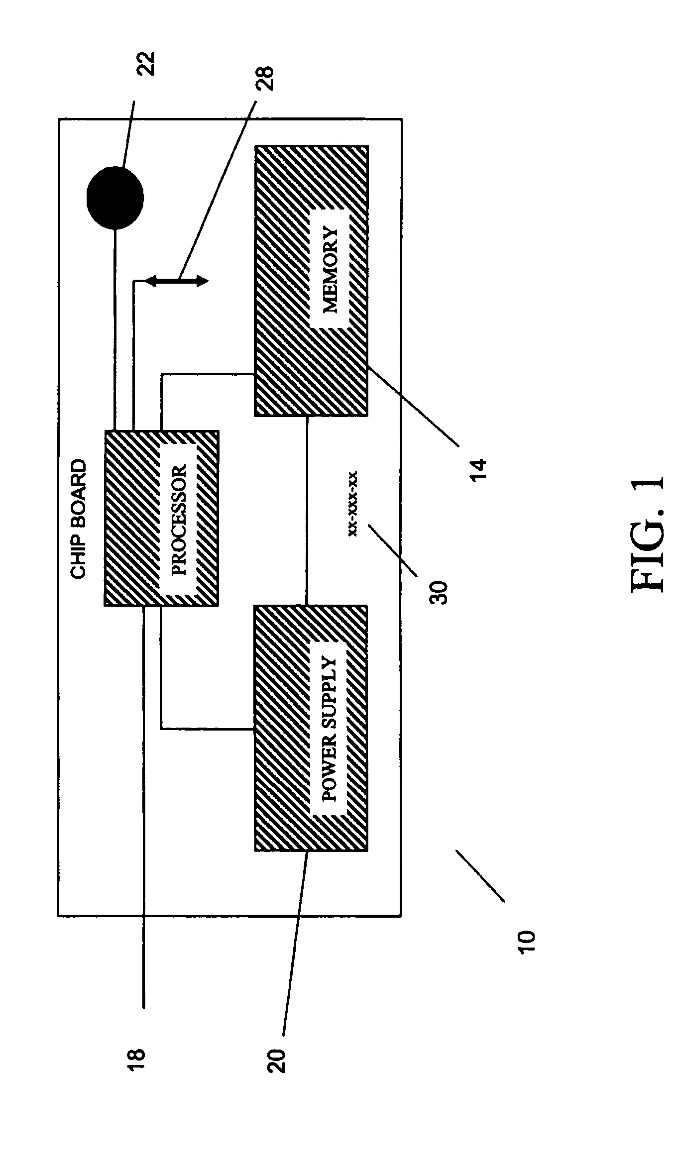
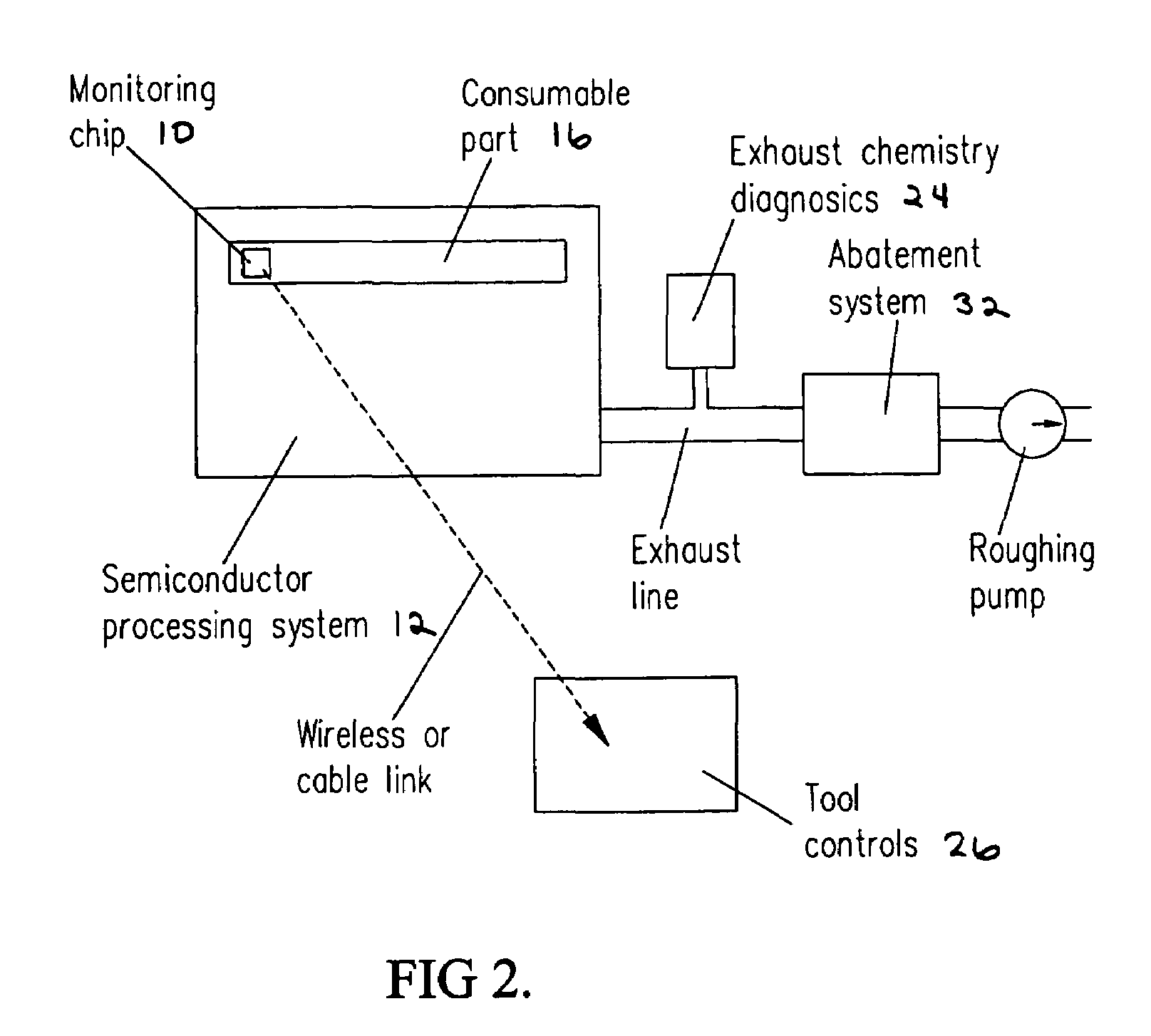
[0021]Referring now to the drawings, FIG. 1 depicts a schematic view of an electronic monitoring device 10 in accordance with one embodiment of the present invention utilized in a semiconductor processing system 12.

[0022]The electronic monitoring device 10 includes a memory 14 dedicated to the consumable part 16 (shown in FIG. 2), which stores a history of chemical exposures of the consumable part 16. The electronic monitoring device 10 includes an electronic monitoring device processor 18 connected to the memory 14, and includes a power supply circuit 20 for providing power to the memory 14 and the processor 18. The memory 14 of the electronic monitoring device 10 is preferably a nonvolatile memory, such as FLASH memory. The power supply circuit 20 can include a power source such as a battery (not shown). The electronic monitoring device 10 can include a gas sensor 22. The processor 18 can transfer data to and from the tool controls 26 (shown in FIG. 2) via a wireless communication...


PUM


Abstract

An electronic monitoring device that archives chemical exposures of a consumable part inside a semiconductor processing tool. The monitoring device includes a memory unit dedicated to the consumable part and which stores a history of the chemical exposures of the consumable part, a processor in communication with the memory unit, and a power supply circuit that supplies power to the processor and the memory unit.

Description

BACKGROUND OF THE INVENTION[0001]1. Field of the Invention[0002]This invention relates to the field of semiconductor processing and more particularly to the securing and disposal of consumable parts from a semiconductor processing tool.[0003]2. Description of the Related Art[0004]In the current semiconductor industry practice, many parts of semiconductor processing apparatus are treated as consumable parts either due to wear on the parts or due to the build up of excessively large film deposits which can contribute to particulate contamination of a semiconductor wafer process.[0005]One example of a consumable part in a semiconductor processing apparatus is a free-standing window insert placed on an interior of a vacuum vessel window. The free-standing window insert protects the vacuum vessel window from, for example, deposits which can build on the vacuum window if unprotected. The free-standing window insert over time is replaced once its optical properties become insufficient for ...

Claims


Application Information

Patent Timeline
Patent Type & Authority Patents(United States)
IPC IPC(8): H01L21/66H01L21/00
CPCH01L21/67253
Inventor CALABRESE, PAULAMITROVIC, ANDREJ
Owner TOKYO ELECTRON LTD
Why Eureka
Try Eureka