Method for monitoring and improving integrated circuit fabrication using FPGAs

a technology of integrated circuits and fabrication processes, applied in the direction of error detection/correction, cad circuit design, instruments, etc., can solve the problems of limited ability to monitor the process, large cost increase, and inability to detect problems occurring in the interior of integrated circuits, etc., to achieve the effect of monitoring and improving the fabrication process of integrated circuits

Active Publication Date: 2006-03-28
XILINX INC
View PDF5 Cites 16 Cited by
  • Summary
  • Abstract
  • Description
  • Claims
  • Application Information

AI Technical Summary

Benefits of technology

[0007]An aspect of the invention is a method for monitoring and improving the fabrication process of integrated circuits using configurable devices. In one aspect, the method includes instantiating a test pattern on one or more configurable devices fabricated using the fabrication process, identifying an underperforming region of the configurable devices, and determining if the un

Problems solved by technology

One challenge in the fabrication of ICs is maintaining and improving yields as the technology changes and improves.
The scribe line, however, is typically less than 10% of the total area, and therefore has limited ability to monitor the process.
In particular, since the scribe line is outside the active chip area, problems occurring in the interior of the integrated circuit, especially highly localized problems, are not detected.
Running a special test wafer greatly increases cost since the test wafer is only used to monitor the process, and will be discarded after serving that purpose.
Typically, such test wafers are only used during development phases of the fabrication process, and not during production

Method used


Image

  • Method for monitoring and improving integrated circuit fabrication using FPGAs
  • Method for monitoring and improving integrated circuit fabrication using FPGAs
  • Method for monitoring and improving integrated circuit fabrication using FPGAs

Examples


Embodiment Construction

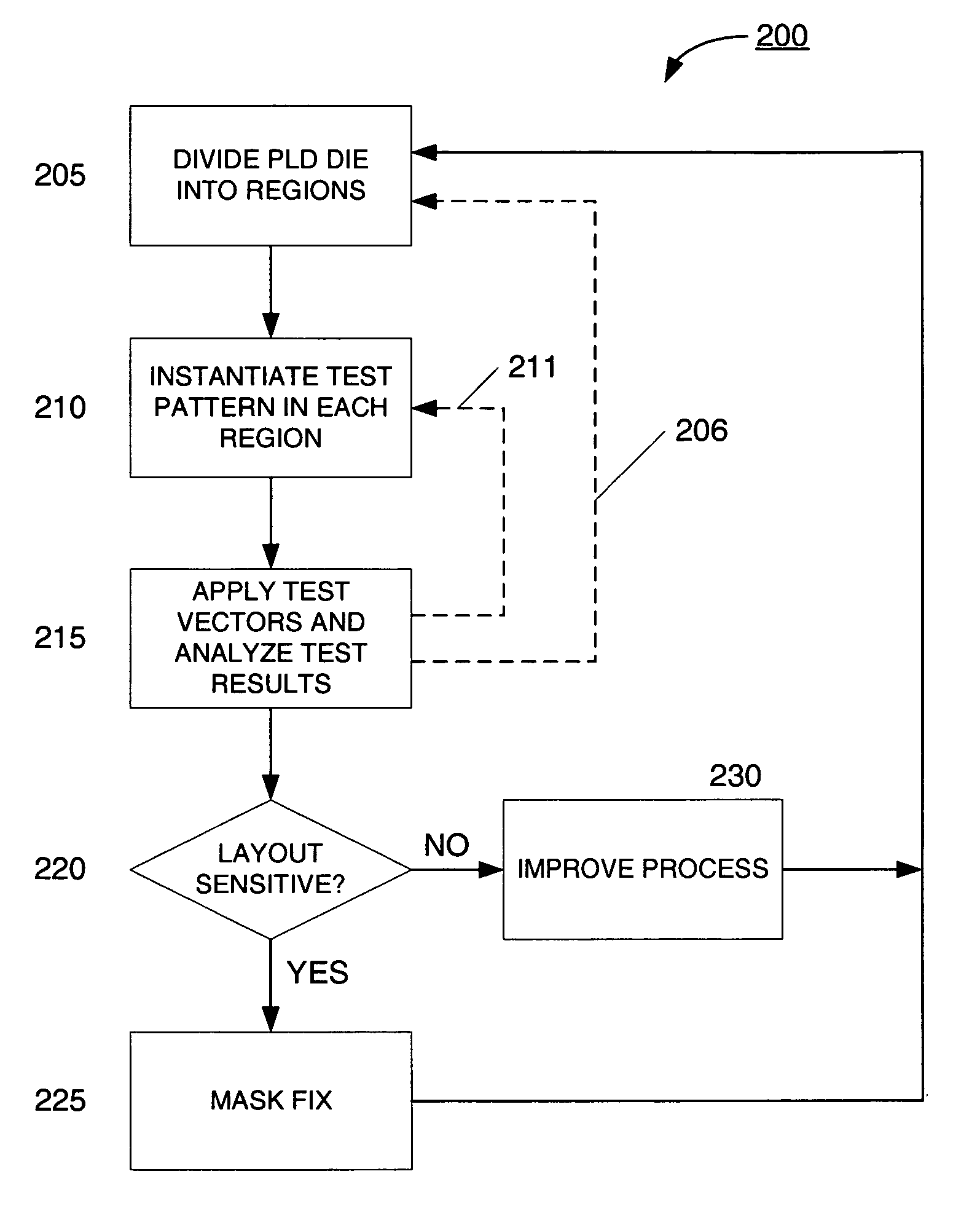
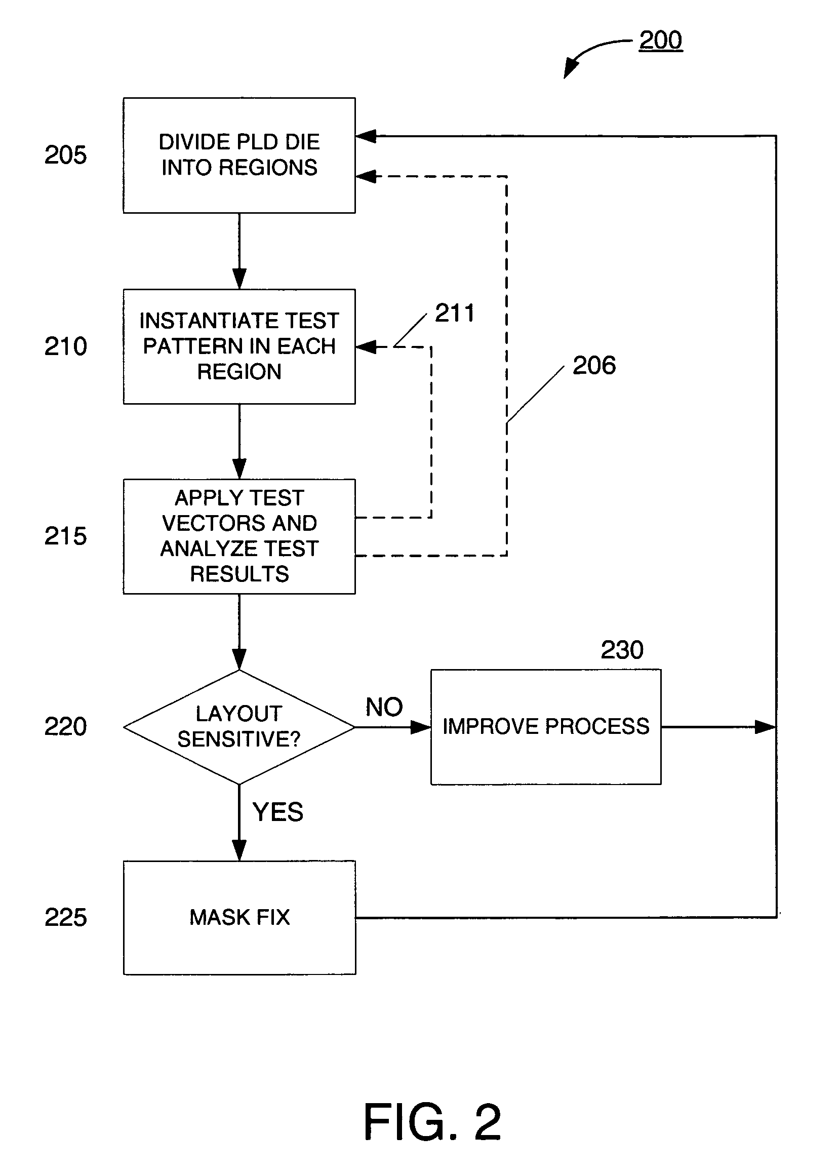
[0016]The present invention is believed to be applicable to a variety of systems for manufacturing, processing and testing integrated circuits. The present invention has been found to be particularly applicable and beneficial for systems including configurable devices such as programmable logic devices having configurable logic blocks. While the present invention is not so limited, an appreciation of the present invention is presented by way of specific examples, in this instance with a programmable logic device having an array of configurable logic blocks. The specific details are set forth to provide a more thorough understanding of the present invention. However, it will be apparent to one ordinarily skilled in the art that the present invention can be practiced without these specific details. In other instances, well-known circuits and devices may be omitted or presented in abstract form in order to avoid obscuring the present invention.

[0017]In accordance with the present inven...


PUM


Abstract

Methods for monitoring and improving the fabrication process of integrated circuits using configurable devices are described. In one aspect, the method includes instantiating a test pattern on one or more configurable devices fabricated using the fabrication process, identifying an underperforming region of the configurable devices, and determining if the underperforming region is layout sensitive. At least one of the fabrication process and the layout of the configurable device can then be adjusted based on the determination. In some embodiments, the configurable device may be a programmable logic device, such as a field programmable logic array.

Description

FIELD OF THE INVENTION[0001]The invention relates to fabrication of integrated circuits, and more particularly, to methods for monitoring and improving fabrication processes for integrated circuits.BACKGROUND OF THE INVENTION[0002]Integrated circuits (ICs) continue to become faster, cheaper and smaller as the fabrication processes for forming ICs improve. One challenge in the fabrication of ICs is maintaining and improving yields as the technology changes and improves. For example, technology improvements may include the use of new materials (such as copper for metal interconnects), or new techniques (such as improved etching and chemical mechanical polishing (CMP) techniques) that may have an impact on the yield of the fabrication process. It is desirable to minimize the effects on yield and thereby improve cost-efficiency.[0003]Prior art methods for monitoring processes and improving yield have some shortcomings. For instance, a “test key,” or a special test circuit, can be placed...

Claims


Application Information

Patent Timeline
IPC IPC(8): G06F17/50
CPCG01R31/318321G06F17/5054G01R31/318519G06F30/34
Inventor ZHAO, JOE W.LI, XIAO-YUWANG, FENGLING, ZHI-MIN
Owner XILINX INC
Why Eureka
Try Eureka