Optimized technology mapping techniques for programmable circuits

Inactive Publication Date: 2006-03-28
ALTERA CORP
View PDF20 Cites 7 Cited by
  • Summary
  • Abstract
  • Description
  • Claims
  • Application Information

AI Technical Summary

Benefits of technology

[0020]If more than one type of merging group can form a feasible programmable logic block, the technology mapping process selects the best merging group for a strategic node by using a cost

Problems solved by technology

The major weakness of this algorithm is that it cannot create a minimal depth macrocell network, though it may reduce area utilization.
The major weakness for

Method used


Image

  • Optimized technology mapping techniques for programmable circuits
  • Optimized technology mapping techniques for programmable circuits
  • Optimized technology mapping techniques for programmable circuits

Examples


Embodiment Construction

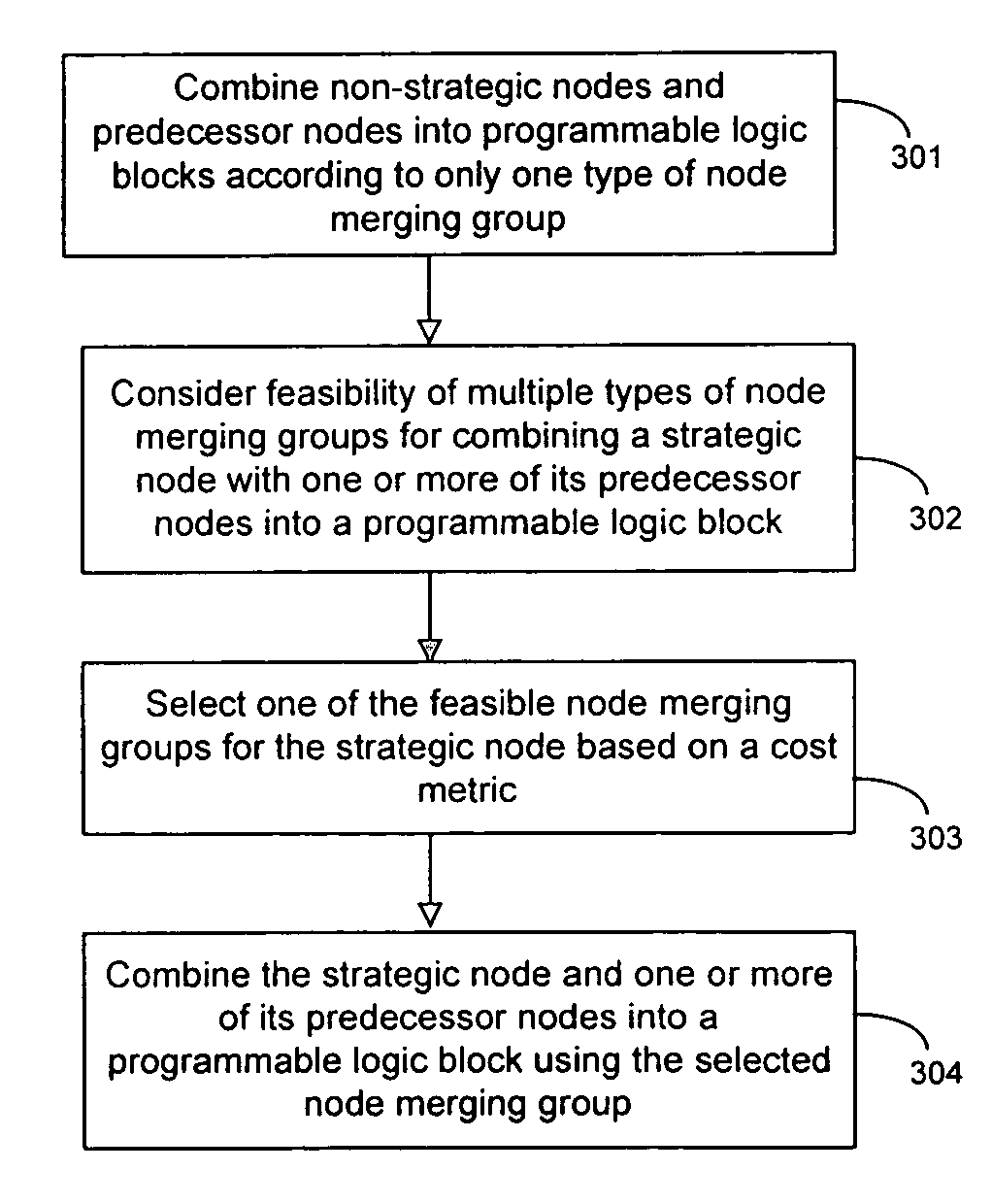
[0040]The present invention involves technology mapping techniques for mapping logic cones to networks of programmable logic blocks. For example, the present invention can be used to map logic cones to networks of macrocells.

[0041]However, the techniques of the present invention are not limited to macrocells. Macrocells are discussed herein merely as one example of a programmable logic block that can be used with the present invention. The technology mapping techniques of the present invention can also be used to map logic cones onto other types of programmable logic blocks that are located in different types of PLD and FPGA architectures. For example, the present invention can be used to map logic cones to logic elements, groups of logic elements called logic array blocks (LABs), and configurable logic blocks.

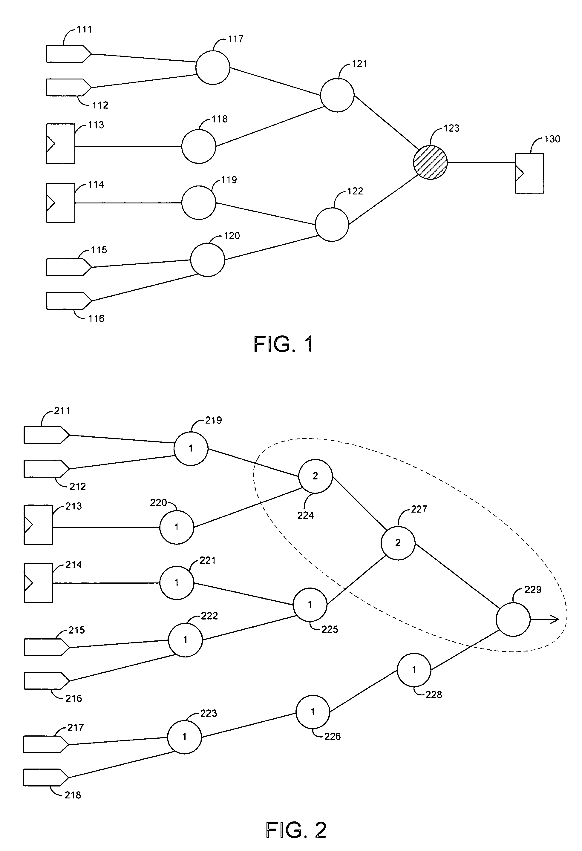
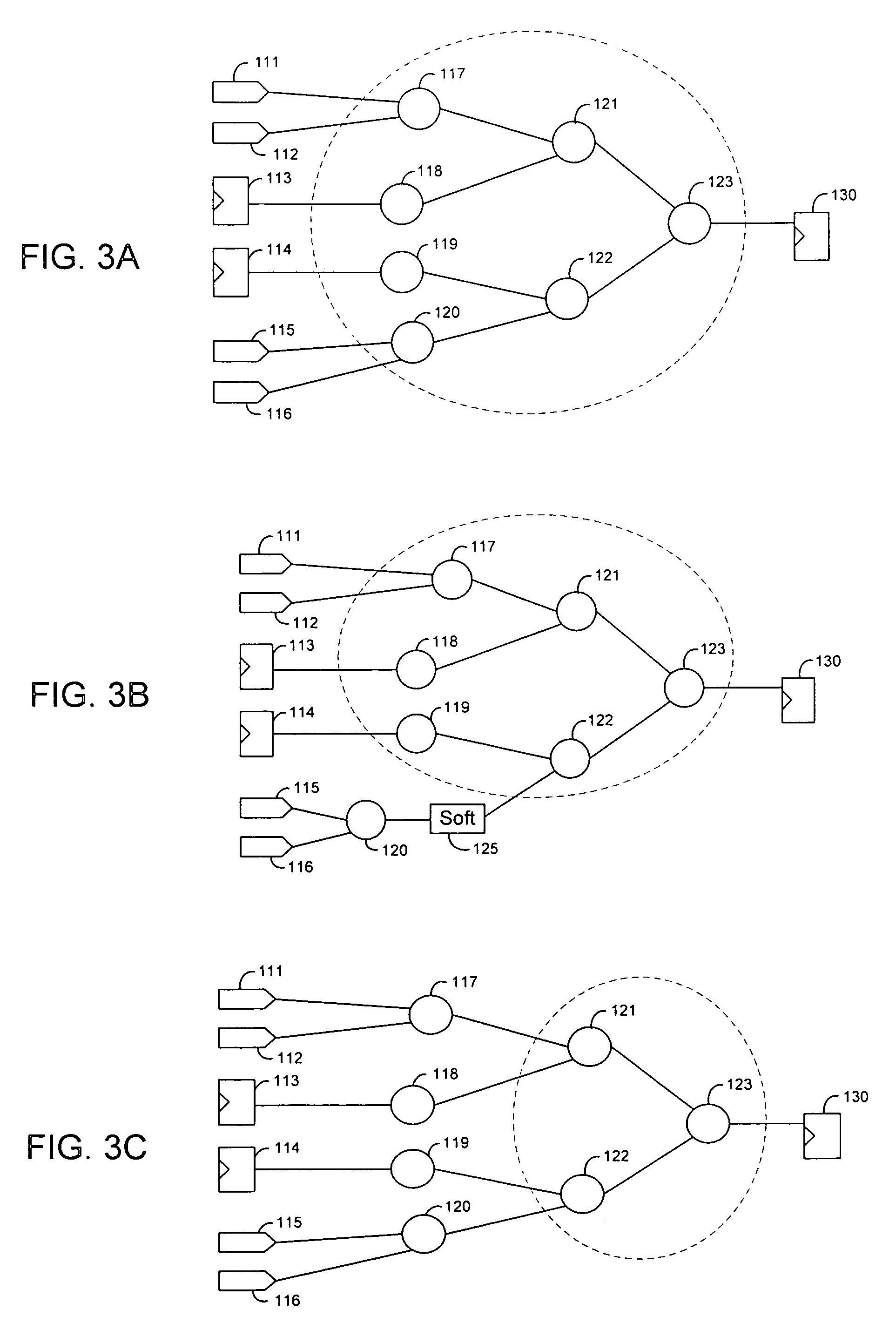
[0042]FIG. 1 illustrates an example of a logic cone. A logic cone is a logic region of a user design for a programmable integrated circuit that lies between one output boundar...


PUM


Abstract

Technology mapping techniques are provided for converting a user design for a programmable integrated circuit to a network of programmable logic blocks. The technology mapping process attempts to combine each non-strategic node and predecessor nodes in one programmable logic block according to only one type of node merging group. If the non-strategic node can be feasibly merged with predecessor nodes according to the merging group, they are grouped into a programmable logic block. The technology mapping process tries to merge strategic nodes with various merging groups of predecessor nodes to form a programmable logic block. The technology mapping process can select the best merging group for the strategic node by using a cost metric. The cost metric can consist of depth and area information of a network for the logic cone.

Description

BACKGROUND OF THE INVENTION[0001]The present invention relates to techniques for mapping a circuit design to a programmable integrated circuit, and more particularly, to efficient technology mapping techniques for programmable integrated circuits.[0002]Programmable integrated circuits can be programmed to implement many types of circuit designs. Examples of programmable integrated circuits include programmable logic devices (PLDs), complex programmable logic devices (CPLDs), field programmable gate arrays (FPGAs), programmable logic arrays (PLAs), and configurable logic arrays (CLAs).[0003]Programmable integrated circuits include numerous programmable logic blocks. Each programmable logic block can be individually configured to implement combinatorial or sequential logic operations.[0004]Altera's MAX family of PLDs are examples of programmable logic devices. Altera MAX devices include numerous programmable logic blocks called macrocells. Each macrocell has a logic array that can be ...

Claims


Application Information

Patent Timeline
IPC IPC(8): G06F17/50
CPCG06F17/5054G06F30/34
Inventor LOONG, LOW YAU
Owner ALTERA CORP
Why Eureka
Try Eureka