
Quantum structure and forming method of the same

a quantum structure and forming method technology, applied in the field of quantum structure, can solve the problems of high supplying voltage, high supplying voltage, and uncertain product life of nvram b>3/b> (the flash ram), and achieve the effect of improving the disadvantages of nvram

Inactive Publication Date: 2006-04-04
UNITED MICROELECTRONICS CORP
View PDF11 Cites 6 Cited by
  • Summary
  • Abstract
  • Description
  • Claims
  • Application Information

AI Technical Summary

Benefits of technology

The present invention provides a method and structure for improving the performance of NVRAM by forming a quantum structure. This method allows for the formation of a quantum structure using existing devices without the need for new ones. Additionally, the method reduces the voltage required for programming and erasing the floating gate, increases the product-life of the NVRAM, and reduces the thickness of the dielectric layer between the floating gate and substrate. The method involves depositing a first dielectric layer, treating it to drive impurities in it to form the quantum structure, and then depositing a second dielectric layer with impurities on top of the first layer.

Problems solved by technology

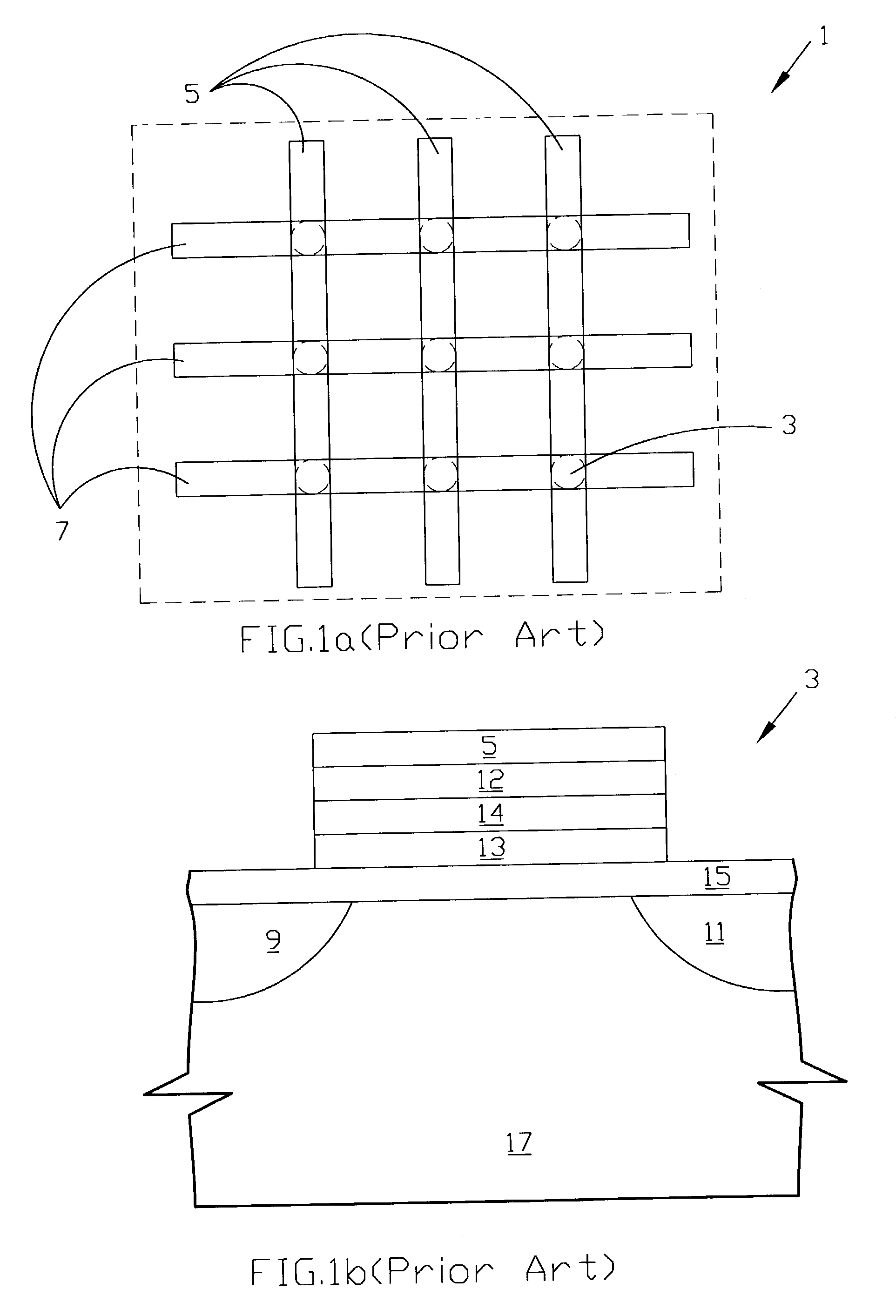
High supplying voltage is the first disadvantage of the traditional NVRAM 3 (the Flash RAM).
The second disadvantage of the NVRAM 3 is the uncertain product-life.
So that it is necessary to improve the disadvantages, i.e. the high supplying voltage, the uncertain product-life and high difficulty for reducing the thickness of the dielectric layer that is deposited between the floating gate and the substrate, of the NVRAM in the prior art.

Method used


Image

  • Quantum structure and forming method of the same
  • Quantum structure and forming method of the same
  • Quantum structure and forming method of the same

Examples


Embodiment Construction

[0019]The preferred embodiments of the present invention that provides a forming method and a structure of a quantum structure according to the difference in characteristic between two matters is described below.

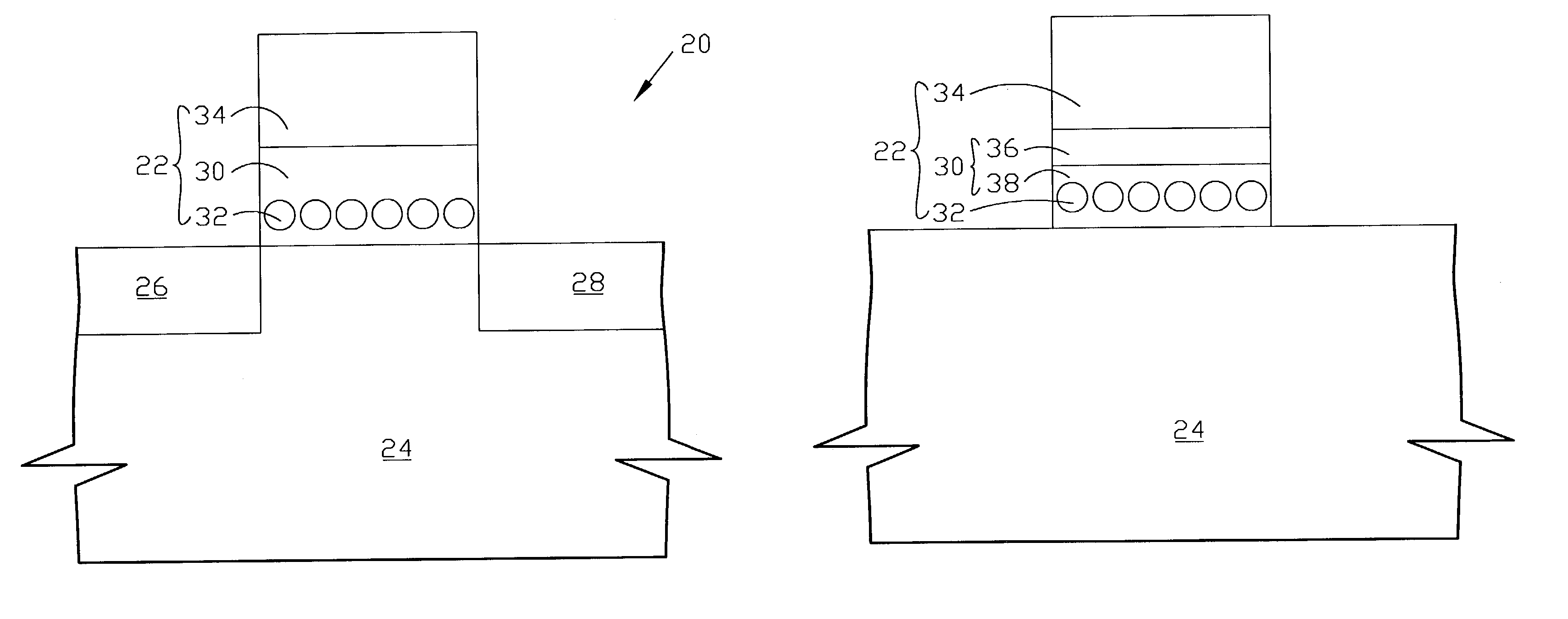
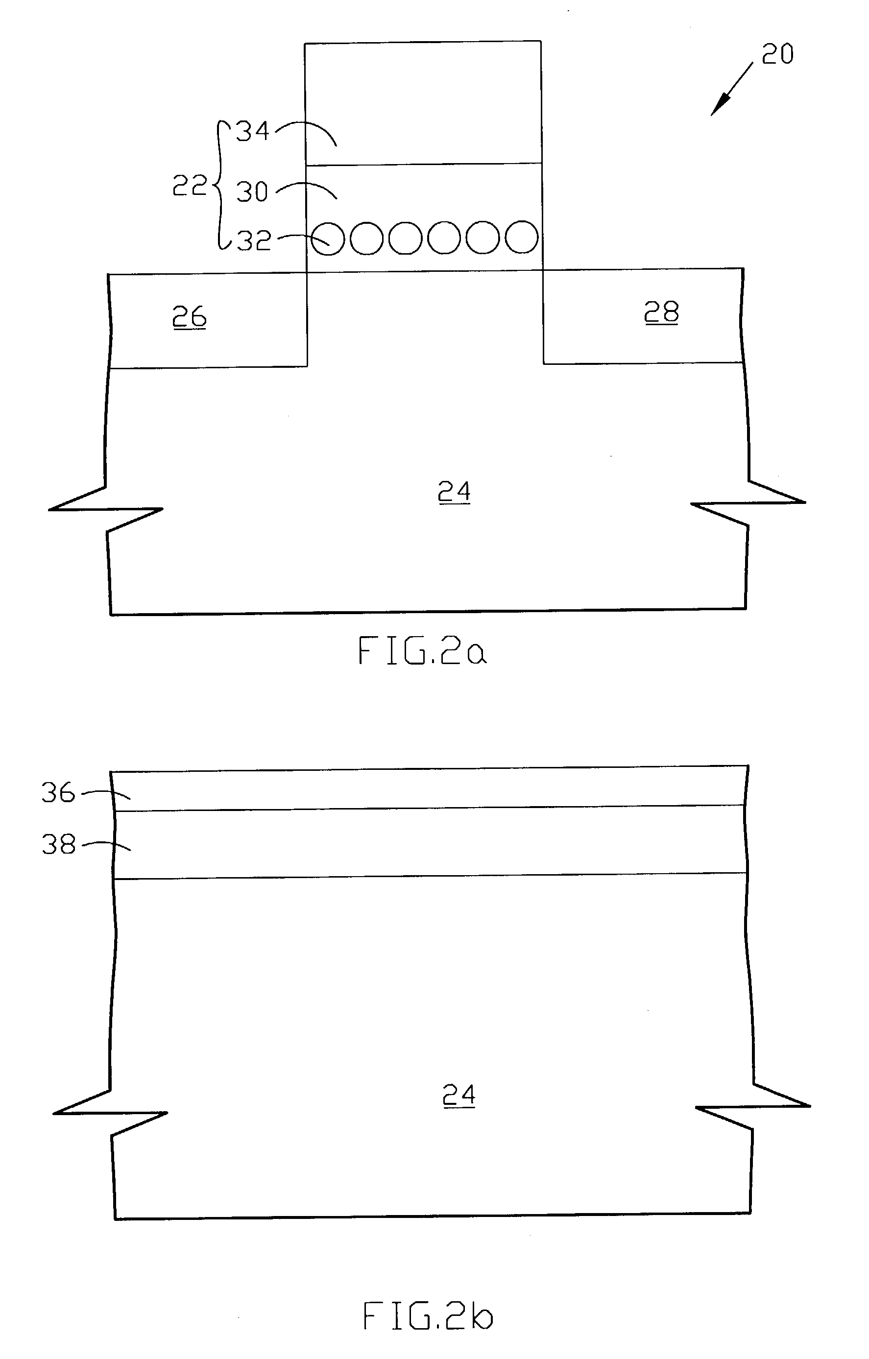
[0020]The method of forming a quantum structure in the present invention comprising several steps. At first, providing a first dielectric layer for forming a second dielectric layer thereon. The second dielectric layer has a plurality of major element and a plurality of impurity contained. Treating the second dielectric layer to drive the impurities to form the quantum structure. For example, oxidizing the major elements to drive the impurities in the first dielectric layer to form the quantum structure in said first dielectric layer because the oxidizing capability of the major elements is stronger than that of the impurities.

[0021]As shown in FIG. 2a, the profile of a NVRAM 20 (non-volatile random access memory) of the first embodiment in the present invention is provided,...


PUM

PropertyMeasurementUnit
supplying voltageaaaaaaaaaa
voltageaaaaaaaaaa
voltageaaaaaaaaaa

Abstract

A quantum structure and the forming method based on the difference in characteristic of two matters is provided. The forming method includes several steps. At first, providing a first dielectric layer for forming a second dielectric layer thereon. The second dielectric layer has major elements and impurities contained. Treating the second dielectric layer to drive the impurities to form the quantum structure. For example, oxidizing the major elements to drive the impurities in the first dielectric layer to form the quantum structure in said first dielectric layer because the oxidizing capability of the major elements is stronger than that of the impurities.

Description

BACKGROUND OF THE INVENTION[0001]1. Field of the Invention[0002]The present invention relates to a quantum structure, and more particularly, to a forming method and a structure of a quantum structure according to the difference in characteristic between two matters.[0003]2. Description of the Prior Art[0004]The NVRAM (non-volatile random access memory) includes many good properties, e.g. little volume, low power consumption, and storing electrical charges by programing and erase. Many technological products depend on the function of NVRAM's to be operated.[0005]A memory cells 1 is shown in FIG. 1a. A plurality of NVRAM 3, e.g. a plurality of Flash RAM, connect with different word lines 5 and bit lines 7, respectively. As shown in FIG. 1b, a profile of the NVRAM 3 is provided. A word line 5 connects to a control gate 12 of a NVRAM 3 and cooperates with a source 9 and a drain 11 to control a floating gate 13 for storing or erasing electrical charges by supplying voltage. The NVRAM 3 c...

Claims


Application Information

Patent Timeline
Patent Type & Authority Patents(United States)
IPC IPC(8): H01L21/336H01L21/28H01L29/423H01L29/51
CPCB82Y10/00H01L21/28185H01L21/28194H01L29/517H01L29/42332H01L29/513H01L21/28273H01L29/40114
Inventor CHANG, TING-CHANGLIU, PO-TSUN
Owner UNITED MICROELECTRONICS CORP
Learn More