

Laminated ceramic capacitor, mounted structure of laminated ceramic capacitor, and capacitor module
a technology capacitor modules, which is applied in the direction of fixed capacitors, stacked capacitors, fixed capacitor details, etc., can solve the problems of difficult control of the temperature rise of laminated ceramic capacitors, difficult to efficiently transfer the heat of internal electrodes, etc., and achieve excellent heat radiation capability
- Summary
- Abstract
- Description
- Claims
- Application Information
AI Technical Summary
Benefits of technology
Problems solved by technology
Method used
Image

Examples
first embodiment
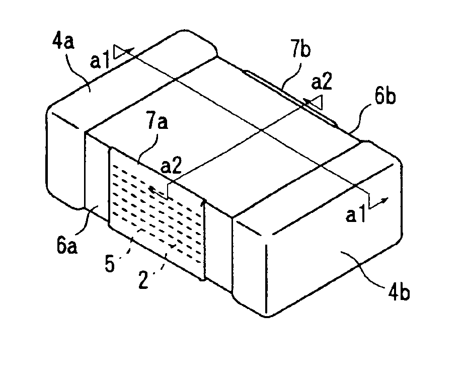
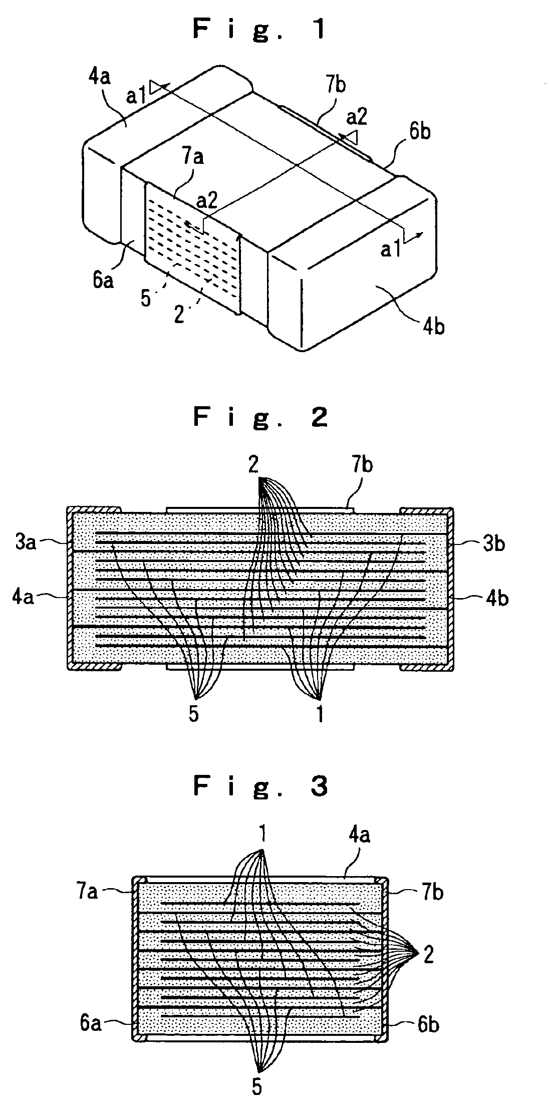
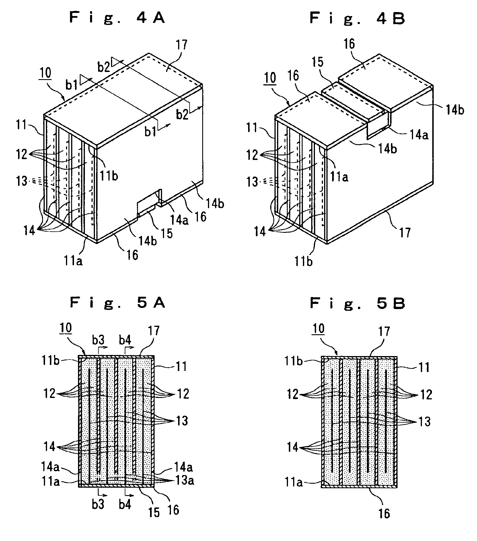
[0091]FIGS. 4 to 7 show the laminated ceramic capacitor.
[0092]Incidentally, FIG. 4A is a perspective view in view of the top face side of the laminated ceramic capacitor, and FIG. 4B is a perspective view in view of the bottom face side of the laminated ceramic capacitor. FIG. 5A is a sectional view taken on line b1—b1 in FIG. 4A, and FIG. 5B is a sectional view taken on line b2—b2 in FIG. 4A. FIG. 6A is a sectional view taken on line b3—b3 in FIG. 5A, and FIG. 6B is a sectional view taken on line b4—b4 in FIG. 5A. FIG. 7A is a diagram where the first electrode, second electrode, and heat radiation conductor are removed from FIG. 4A, and FIG. 7B is a diagram where the first electrode, second electrode, and heat radiation conductor are removed from FIG. 4B.
[0093]This laminated ceramic capacitor 10 comprises a laminated chip 11 with a rectangular parallelepiped shape. This laminated chip 11 has the structure that a plurality of first conductor layers 13 (four in the figure), and a plu...
second embodiment
[0127]FIG. 24 shows the laminated ceramic capacitor.
[0128]Incidentally, FIG. 24 includes a laminated ceramic capacitor 20, a laminated chip 21, a bottom face 21a of the laminated chip, a top face 21b of the laminated chip, ceramic layers22, first conductor layers 23, lead sections 23a, second conductor layers 24, lead sections 24a, a first electrode 25, a second electrode 26, and a heat radiation conductor 27.
[0129]The difference between this laminated ceramic capacitor 20 and the above-mentioned laminated ceramic capacitor 10 is that the numbers of the first electrode 25 and second electrode 26 are made one and one respectively, and the numbers of the lead sections 23a and 24a of respective conductor layers 23 and 24 are made one and one respectively.
[0130]According to this laminated ceramic capacitor 20, it is possible to obtain the same radiating effect as the above-mentioned laminated ceramic capacitor 10 by directly and efficiently transferring the heat of the respective second...
third embodiment
[0131]FIG. 25A shows the laminated ceramic capacitor.
[0132]Incidentally, FIG. 25A includes a laminated ceramic capacitor 30, a laminated chip 31, a bottom face 31a of the laminated chip, a top face 31b of the laminated chip, ceramic layers 32, first conductor layers 33, second conductor layers 34, a first electrode 35, a second electrode 36, and a heat radiation conductor 37.
[0133]The difference between this laminated ceramic capacitor 30 and the above-mentioned laminated ceramic capacitor 10 is that the second conductor layer located in one side face in the laminated direction of conductor layers of the laminated chip 31 is eliminated, and the ceramic layer 32 is exposed on the side face thereof.
[0134]According to this laminated ceramic capacitor 30, it is possible to obtain the same radiating effect as the above-mentioned laminated ceramic capacitor 10 by directly and efficiently transferring the heat of the respective second conductor layers 34 to the heat radiation conductor 37....
PUM
| Property | Measurement | Unit |
|---|---|---|
| Time | aaaaa | aaaaa |
| Electrical conductor | aaaaa | aaaaa |
Abstract
Description
Claims
Application Information