Method of optimizing the timing between signals

a timing and signal technology, applied in the direction of noise figure or signal-to-noise ratio measurement, pulse technique, instruments, etc., can solve the problems of prohibiting multiple employment or usage, complex too complex and space-consuming dynamic clock alignment circuits, etc., to achieve stable and reliable, less space-consuming

Inactive Publication Date: 2006-04-04
POLARIS INNOVATIONS LTD
View PDF2 Cites 7 Cited by
  • Summary
  • Abstract
  • Description
  • Claims
  • Application Information

AI Technical Summary

Benefits of technology

[0004]It is therefore an object of the present invention to provide a method of optimizing the timing between signals which is inherently stable and reliable and which can be at the same time realized by a comparable simple and less space-consuming semiconductor circuitry.SUMMARY OF THE INVENTION
[0014]According to a preferred embodiment of the inventive method of optimizing the timing between signals and according to a further best mode for carrying out the invention a set of consecutively or strictly monotonically ordered test timings and delay test values is used. This in particular simplifies the process of sweeping through the set of possible delay test values.
[0018]It is of further advantage when according to a further embodiment of the present invention and according to a further best mode for carrying out the present invention n is chosen to be 1 in order to achieve at least approximately synchronicity between signals on said sample signal line and said clock signal of said clock delay line.
[0029]A big advantage of this circuit, as compared to a DLL / PLL method is that the circuit can be used for smaller granularities of signals. For example, if 16 signals need to be aligned to one clock, a typical DLL solution would align the clock to the center signal. The problem is that it is difficult to align the other 15 signals to the center signal, thus leading to another source of skew. The invented circuit, on the other hand, is very simple and compact so that it can be used at multiple locations, for instance every 4 or 8 signals, thus reducing the skew within the signal groups. A DLL / PLL is simply too large and power consuming to use multiple times.

Problems solved by technology

However, in doing so the respective circuitry arrangements become comparable complex as such circuitry arrangements are built up for instance as dynamic clock alignment circuits which use delay locked loops DLL or phase locked loops PLL in each case with a dynamic feedback arrangement.
In particular the involved DLL circuits and the PLL circuits and the respective dynamic feedback loops make the dynamic clock alignment circuits too complex and too area space-consuming and therefore prohibit a multiple employment or usage of such circuits within a given semiconductor circuitry.

Method used


Image

  • Method of optimizing the timing between signals
  • Method of optimizing the timing between signals
  • Method of optimizing the timing between signals

Examples


Embodiment Construction

[0037]In the following elements and structures with similar or equivalent functionalities will be described and denoted by the same reference symbols. Not in each case of their occurrence a detailed description thereof is repeated.

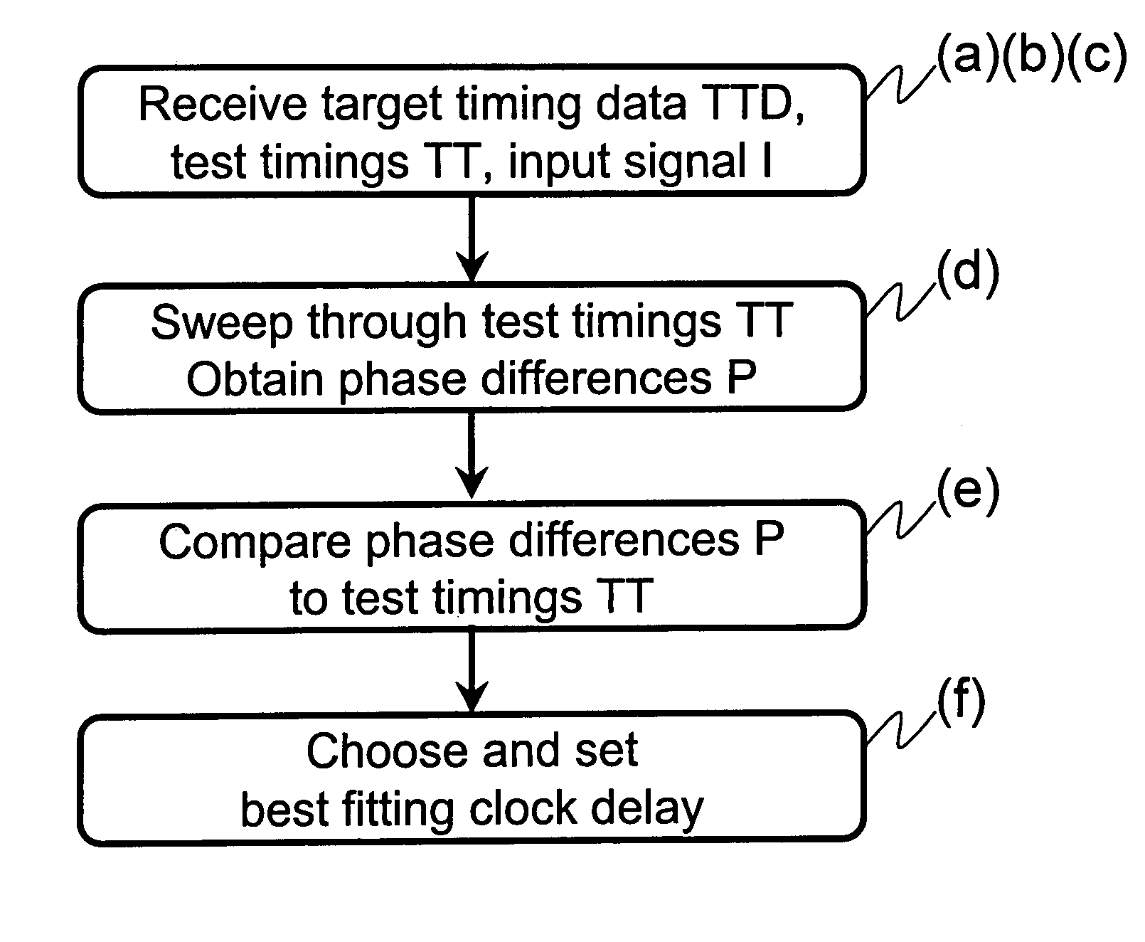
[0038]FIG. 1 is a schematic block diagram describing a first embodiment of the present invention in the sense of a method of optimizing the timing between signals to be latched and a respective latching clock signal.

[0039]A first subprocess of receiving a target timing data TTD, the test timings TT as well as the test input signal I unifies the steps (a), (b), and (c) of the present invention. It follows a step (d) in which a process of sweeping through the test timings and the respective delay test values is realized and in which the respective phase differences between the test input signal I as a sample signal and the respective clock signals C are measured. In a following step (e) the obtained phase differences P are compared to the target timing data ...


PUM


Abstract

A method of optimizing the timing between signals to be latched and a respective latching clock signal is suggested wherein test timings are provided according to which a delay test value of a clock delay line (CDL) are generated. According to the delay test values a clock signal (C) and a sample signal (S) are received through said clock delay line (CDL) and through said sample signal line (SSL), respectively. Respective phase differences for the distinct delay test values are obtained. A delay value is chosen and set for operation for which the respective obtained phase difference fits best to given target timing data.

Description

FIELD OF THE INVENTION[0001]The present invention relates to a method of optimizing the timing between signals and in particular to a method of optimizing the timing between signals to be latched and a respective latching clock signal with respect to a given circuitry arrangement. The present invention further relates to a method for latching received signals as well as to an apparatus for optimizing the timing between signals.BACKGROUND OF THE INVENTION[0002]Synchronous signals which are transferred to a semiconductor circuitry arrangement and in particular to a memory chip or the like are often subject of a storing process or latching process. Such a storing process or latching process for instance in memory chip applications is initialized and ruled by respective clock signals. After receiving e.g. multiple synchronous signals from external the respective synchronous signals to be latched and the respective latching signal or latching clock signal may suffer different delay proce...

Claims


Application Information

Patent Timeline
Patent Type & Authority Patents(United States)
IPC IPC(8): G01R35/00G01R13/00H03K5/00H03K5/135H03K5/159
CPCH03K5/135H03K2005/00104H03K2005/00084
Inventor NYGREN, AARON JOHN
Owner POLARIS INNOVATIONS LTD
Why Eureka
Try Eureka