
Circuitry for arithmetically accumulating a succession of arithmetic values

a technology of arithmetic value and circuit, applied in the field of function-specific blocks, can solve the problems of “more expensive” to use a global interconnection conductor than a local interconnection conductor, and the slowness of global interconnection conductors, so as to reduce the impact of including fsbs, resource input may reduce or even sacrifice the usability of other resources

Inactive Publication Date: 2006-04-04
ALTERA CORP
View PDF28 Cites 14 Cited by
  • Summary
  • Abstract
  • Description
  • Claims
  • Application Information

AI Technical Summary

Benefits of technology

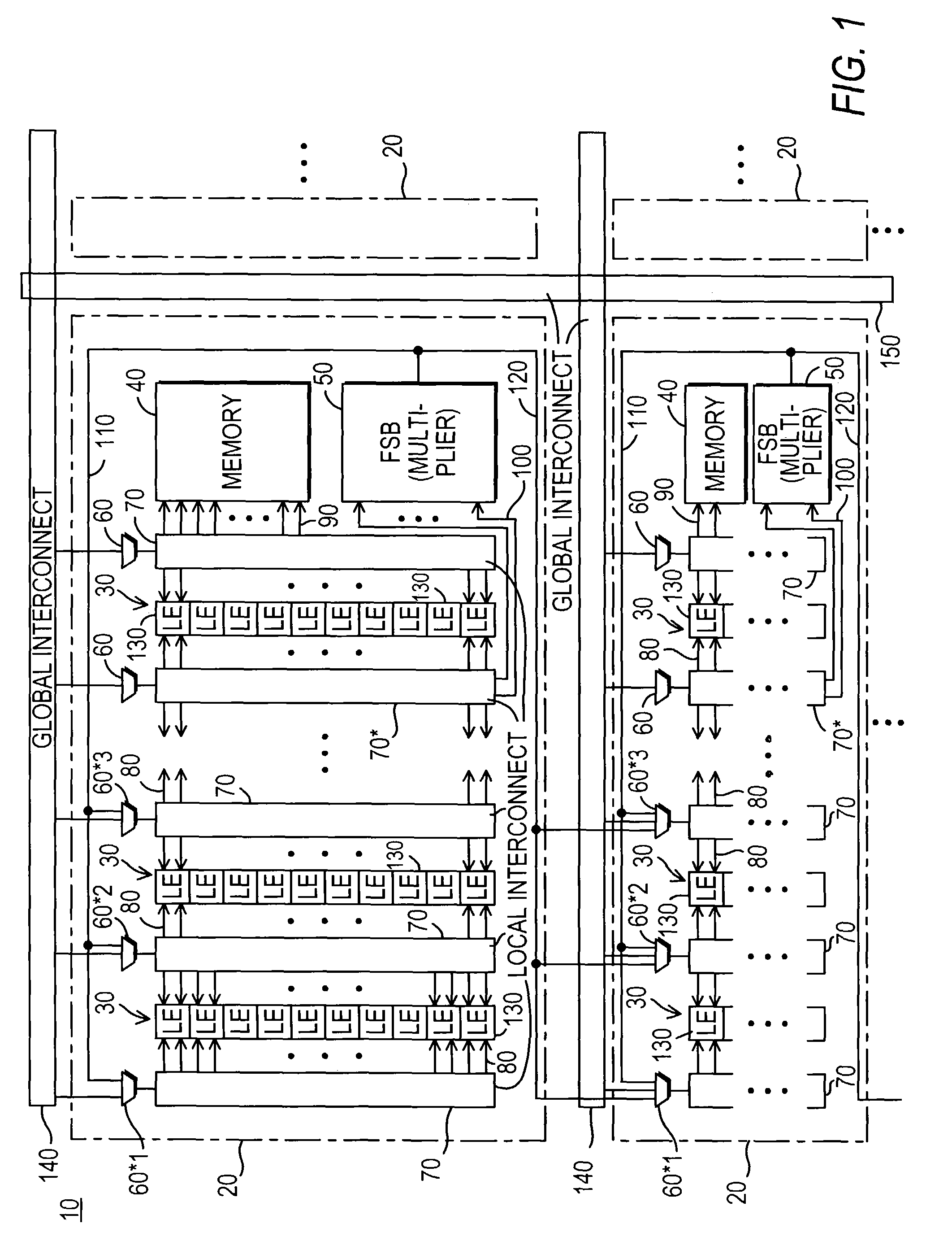
[0008]In order to reduce the impact of including FSBs on the interconnection resources of the PLD, any or all of several techniques respecting the interconnection resources may be used in accordance with this invention. One technique is to derive inputs for the FSB from interconnection resources that are already fairly local (i.e., close) to the inputs of other resources such as logic regions (or memory regions if memory regions are included (although borrowing inputs from logic is presently preferred)). In this way the FSB effectively shares substantial amounts of input routing resources with those other (logic / memory / etc.) resources. A smaller fraction of the overall interconnection resources must be dedicated to providing FSB inputs, and the impact on use of the more global (as opposed to the local) interconnection resources is especially reduced. (Global interconnection resources include relatively long interconnection conductors, in contrast to the relatively short conductors that can be used for more local interconnections. Accordingly, it is “more expensive” to use a global interconnection conductor than a local interconnection conductor. Also, global interconnection conductors tend to be slow and to require drive by power-consuming drivers, whereas local conductors tend to be faster and may not require additional drivers.) Sharing an interconnection resource between an FSB input and another logic / memory / etc. resource input may reduce or even sacrifice the usability of the other resource when the PLD is configured to use the FSB, but that can be preferable to having to provide more interconnection resources that are dedicated to providing FSB inputs.
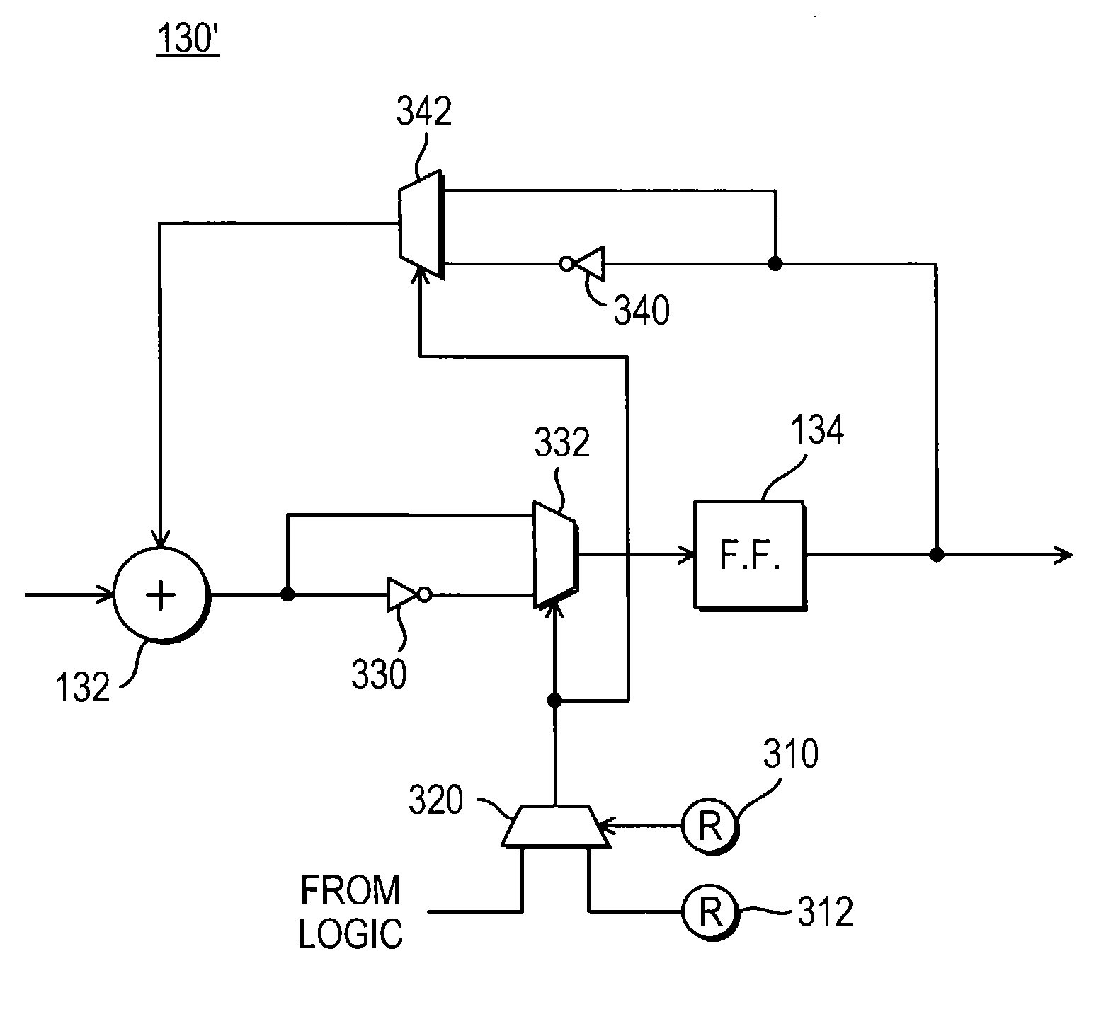
[0009]Another technique that can be used to reduce the impact of an FSB on the interconnection resources of a PLD is to use relatively local interconnection resources for the outputs of the FSB. These local resources can be used to supply the FSB outputs to the inputs (or other relatively local interconnection resources leading to the inputs) of particular subsets of other resources such as logic regions on the PLD. This avoids the need for drivers and / or more global interconnection conductors dedicated to the FSB outputs. If FSB output driving by drivers is needed, the output drivers of the immediately above-mentioned logic regions can be used. Similarly, if the FSB outputs need registering, the registers of these logic regions can be used. And these logic regions can even be used to at least begin further logical and / or arithmetic manipulation of the FSB outputs. Once again, this effective sharing of certain FSB output functions with logic regions may reduce or sacrifice the usefulness of those logic regions for other purposes when the FSB is being used, but that can be preferable to having to provide more dedicated interconnection resources to support the FSB.

Problems solved by technology

Accordingly, it is “more expensive” to use a global interconnection conductor than a local interconnection conductor.
Also, global interconnection conductors tend to be slow and to require drive by power-consuming drivers, whereas local conductors tend to be faster and may not require additional drivers.)

Method used


Image

  • Circuitry for arithmetically accumulating a succession of arithmetic values
  • Circuitry for arithmetically accumulating a succession of arithmetic values
  • Circuitry for arithmetically accumulating a succession of arithmetic values

Examples


Embodiment Construction

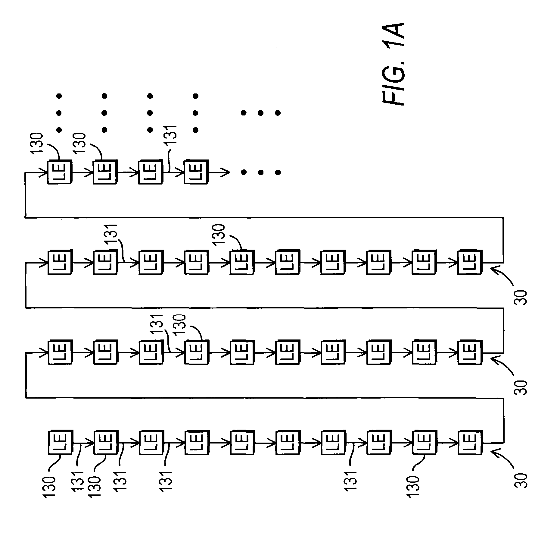
[0035]The invention will be at least initially described with greatest emphasis on inclusion of parallel multipliers in PLDs, but other examples of FSBs will also be mentioned and described, and from the overall disclosure it will be apparent to those skilled in the art how the invention can be applied to any of many different types and constructions of FSBs.

[0036]The illustrative PLD 10 shown in FIG. 1 includes a two-dimensional array of intersecting rows and columns of “super-regions”20 of programmable logic and other resources. Each super-region 20 includes a plurality of “regions”30 of programmable logic, a region 40 of memory, and an FSB50, which in this example is dedicated (i.e., at least partly hard-wired) parallel multiplier circuitry. Each super-region 20 also includes some relatively local interconnection resources such as programmable logic connectors (“PLCs”) 60, the regions of interconnection conductors and PLCs labeled 70, logic-element-feeding conductors 80, memory-r...


PUM


Abstract

A programmable logic integrated circuit device has at least one function-specific circuit block (e.g., a parallel multiplier, a parallel barrel shifter, a parallel arithmetic logic unit, etc.) in addition to the usual multiple regions of programmable logic and the usual programmable interconnection circuit resources. To reduce the impact of use of the function-specific block (“FSB”) on the general purpose interconnection resources of the device, inputs and / or outputs of the FSB may be coupled relatively directly to a subset of the logic regions. In addition to conserving general purpose interconnect, resources of the logic regions to which the FSB are connected can be used by the FSB to reduce the amount of circuitry that must be dedicated to the FSB. If the FSB is a multiplier, additional features include facilitating accumulation of successive multiplier outputs (using either addition or subtraction and with sign extension if desired) and / or arithmetically combining the outputs of multiple multipliers.

Description

[0001]This application is a divisional of U.S. nonprovisional patent application Ser. No. 09 / 924,354, filed Aug. 7, 2001 (now U.S. Pat. No. 6,628,140), which claims the benefit of U.S. provisional patent application No. 60 / 233,389, filed Sep. 18, 2000, each of which is hereby incorporated by reference herein in its entirety.BACKGROUND OF THE INVENTION[0002]This invention relates to programmable logic integrated circuit devices, and more particularly to function-specific blocks such as multipliers, arithmetic logic units, barrel shifters, and / or the like in programmable logic devices.[0003]Programmable logic devices (“PLDs”) are well known as is shown, for example, by Jefferson et al. U.S. Pat. No. 6,215,326 and Ngai et al. U.S. Pat. No. 6,407,576. PLDs typically include many regions of programmable logic that are interconnectable in any of many different ways by programmable interconnection resources. Each logic region is programmable to perform any of several logic functions on inp...

Claims


Application Information

Patent Timeline
IPC IPC(8): G06F7/50G06F5/01H01L21/82G06F7/48G06F7/509G06F7/52G06F7/53G06F7/575G06F7/72G06F15/78H03K19/173H03K19/177
CPCG06F7/5095H03K19/17736G06F15/7867H03K19/177H03K19/17732G06F5/015G06F7/53G06F7/575G06F2207/3828G06F7/724
Inventor LANGHAMMER, MARTINPRASAD, NITIN
Owner ALTERA CORP
Learn More