Architecture for efficient implementation of serial data communication functions on a programmable logic device (PLD)

a programmable logic and serial data technology, applied in data switching networks, instruments, pulse techniques, etc., can solve the problems of inflexibility, high cost, and inflexibility of approaches, and achieve the effect of small and/or faster operation

Inactive Publication Date: 2006-04-04
MONTEREY RES LLC
View PDF71 Cites 20 Cited by
  • Summary
  • Abstract
  • Description
  • Claims
  • Application Information

AI Technical Summary

Benefits of technology

[0016]The present invention includes an integrated circuit having a programmable portion and a communication portion. A programmable portion may include user configurable gates, such as those in conventional programmable logic devices (PLD). A communication portion may include circuits designed to perform predetermined comm

Problems solved by technology

While fully custom application specific integrated circuits (ASICs) can be developed to meet a particular application, such approaches may be expensive and inflexible.
Such approaches can incur expenses, as manufacturing components (e.g., masks, packaging etc.) may have to be custom developed for the ASIC.
Such approaches may be inflexible, as changes in a design can be difficult to accommodate without altering existing manufacturing components.
A drawback to such conventional approaches can be the gate “cost” of realizing such serial communication functions on a PLD.
Dedicating such a numbe

Method used


Image

  • Architecture for efficient implementation of serial data communication functions on a programmable logic device (PLD)
  • Architecture for efficient implementation of serial data communication functions on a programmable logic device (PLD)
  • Architecture for efficient implementation of serial data communication functions on a programmable logic device (PLD)

Examples


Embodiment Construction

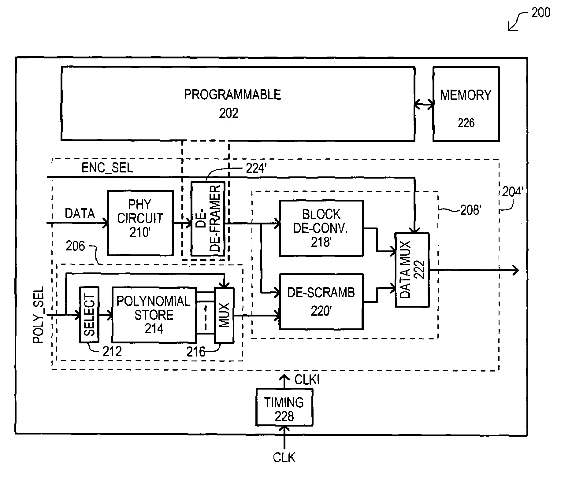
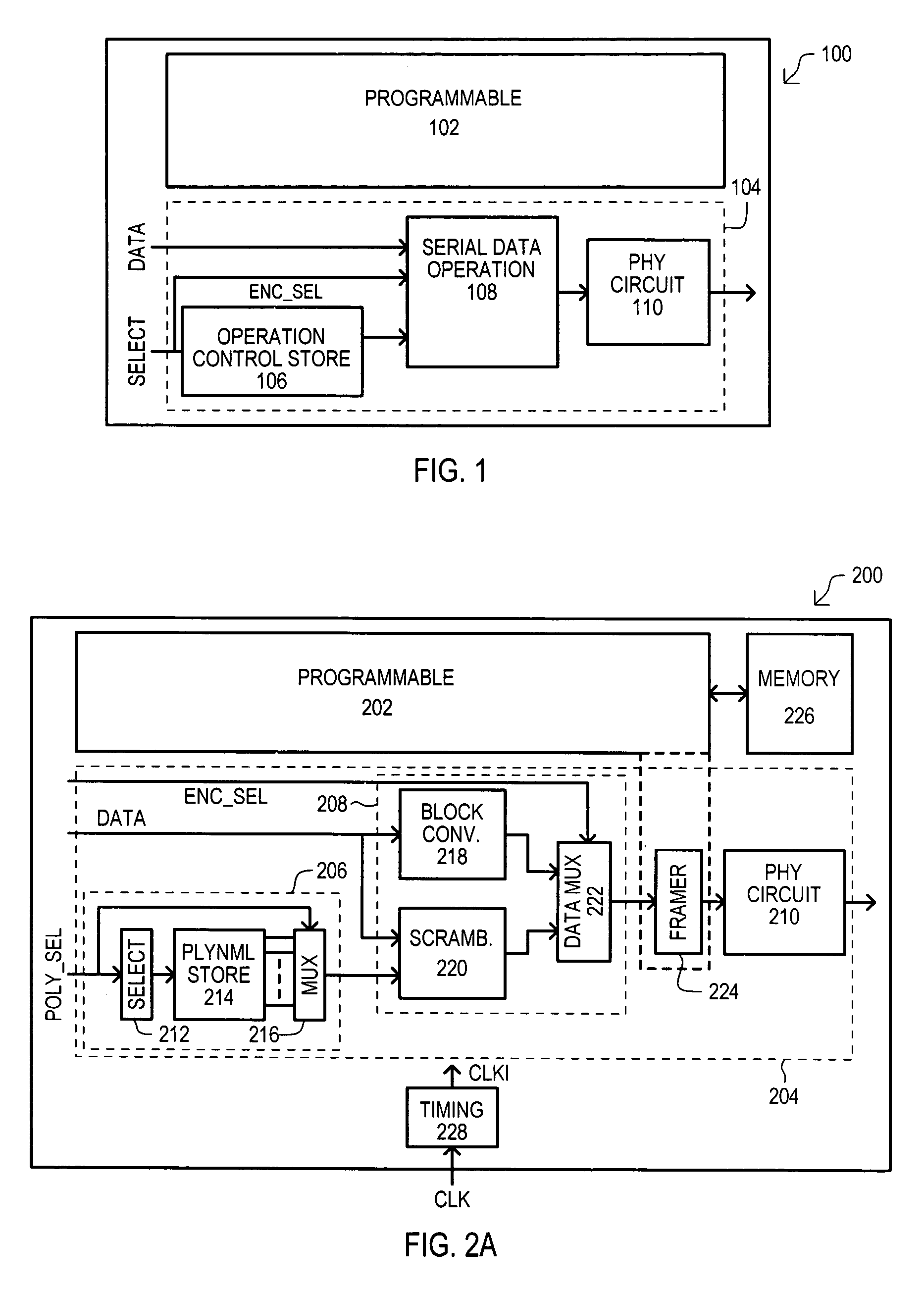
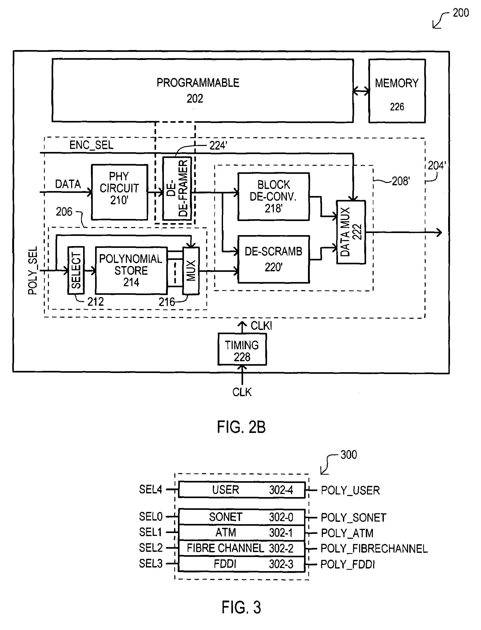
[0025]Various embodiments will now be described in conjunction with a number of diagrams. The embodiments set forth a programmable logic device (PLD) that may include circuits dedicated to one or more particular serial communication functions. All, or a portion of such circuits may be formed specifically for such functions, as opposed to being configured by a conventional design and synthesis process. Serial data values may be received, and operated on according to variables that are hardwired or programmed into the device. Different variables are selectable to enable different applications, such as encoding / de-coding and / or scrambling / de-scrambling.

[0026]Referring now to FIG. 1, an integrated circuit (IC) according to a first embodiment is set forth in a block diagram and designated by the general reference character 100. An IC 100 may include a programmable portion 102 and a communication portion 104. A programmable portion 102 may include programmable logic circuits that may be c...


PUM


Abstract

According to one embodiment, an integrated circuit (100) includes a programmable portion (102) and a communication portion (104). A programmable portion (102) may include logic circuits that are configurable by a user. A communication portion (104) may include one or more circuit blocks designed to perform predetermined serial data communication functions. According to one embodiment, a communication portion (104) may include a block converter (218) that can encode/decode input data words into output data words, and a scrambler circuit (220) for scrambling/de-scrambling data according to a predetermined scrambling polynomial value. Different scrambling polynomial values may be selected from an operation control store (206) to provide a variety of different scrambling/de-scrambling functions. The inclusion of a communication portion (104) may reduce the size and/or increase the speed of an integrated circuit over conventional approaches that may synthesize serial data communication functions from programmable logic circuits.

Description

TECHNICAL FIELD[0001]The present invention relates generally to programmable logic devices (PLDs), and more particularly to PLDs that may be configured for data communication applications.BACKGROUND OF THE INVENTION[0002]Programmable logic has increasingly become a valued resource for system designers. Programmable logic can allow for a custom logic design to be implemented without the initial cost, delay and complexity of designing and fabricating an application specific integrated circuit (ASIC).[0003]Currently, there are many variations of programmable logic, including simple programmable logic devices (SPLDs), complex PLDs (CPLDs), and field programmable gate arrays (FPGAs) (referred to herein collectively as programmable logic devices (PLDs)).[0004]While PLDs can have numerous applications, one application of increasing value is serial data communications. Increasingly, various electronic devices can communicate with one another with serial data streams of various protocols. A ...

Claims


Application Information

Patent Timeline
IPC IPC(8): G06F17/50G06F15/177G06F9/00H01L25/00H04L12/66
CPCH03K19/17744H03K19/17732H03K17/002
Inventor MOORE, MICHAEL T.LIE, JAMES
Owner MONTEREY RES LLC
Why Eureka
Try Eureka