Light emitting device and manufacturing method thereof
a technology of light emitting device and manufacturing method, which is applied in the direction of discharge tube luminescnet screen, discharge tube/lamp details, electric discharge lamp, etc., to achieve uniform color and luminance distribution
- Summary
- Abstract
- Description
- Claims
- Application Information
AI Technical Summary
Benefits of technology
Problems solved by technology
Method used
Image

Examples
first embodiment
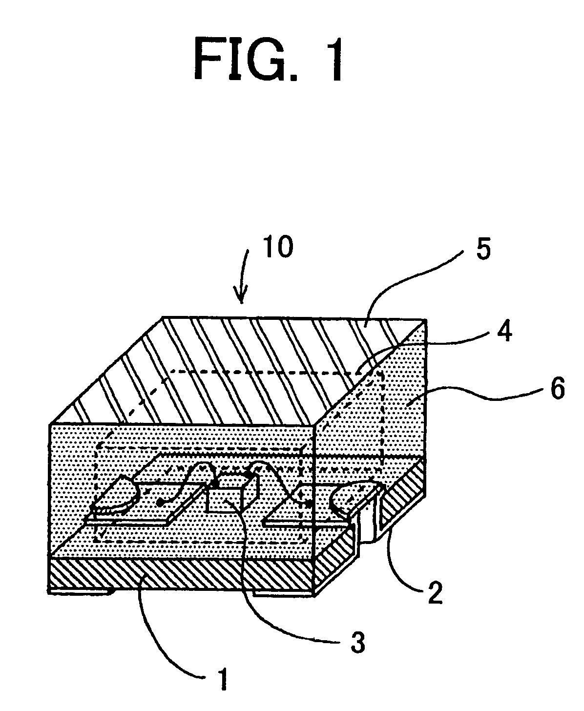
[0021]Referring to FIG. 1 showing a perspective view of a light emitting device according to the present invention, the light emitting device 10 comprises a substrate 1 made of an insulation material such as an epoxy resin, a pair of opposite electrodes 2, each of which extends to the underside of the substrate as a terminal, an LED 3 mounted on the substrate and connected to the electrodes 2 by wire bonding.
[0022]The LED 3 is composed to emit blue light. The LED 3 is sealed by a first sealing cubic transparent layer 4 made of a transparent resin such as epoxy resin. The first transparent layer 4, in turn is covered by a second parallelpiped transparent layer 5 made of transparent resin such as epoxy resin. In the second transparent layer 5, particles of fluorescence material such as yttrium aluminum garnet (YAG), and particles of coloring agent are included. Outside walls of the second transparent layer 5 except the upper side are covered by a reflector layer 6 by metal plating of ...
second embodiment
[0028]Referring to FIG. 3 showing a sectional view of a light emitting device according to the present invention, the same parts as FIG. 1 are identified with the same reference numeral as FIG. 1, and the explanation of the parts is omitted.
[0029]A condenser lens portion 4a is formed on the surface of the first transparent layer 4. The condenser lens portion 4a condenses the light from the LED 3, thereby increasing the luminance of the emitted light.
third embodiment
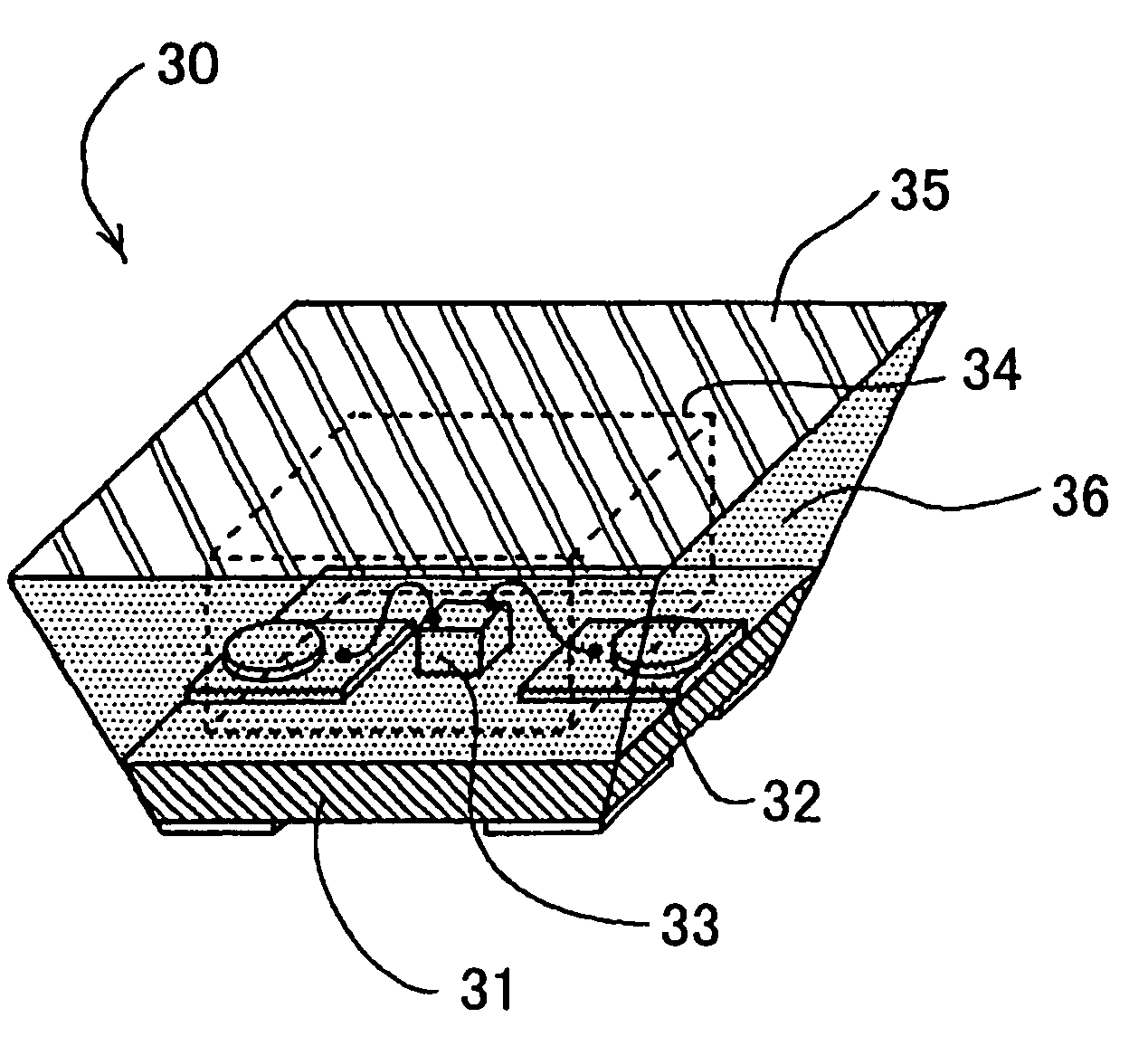
[0030]the light emitting device of the present invention will be described with reference to FIG. 4.
[0031]The light emitting device 30 comprises a substrate 31 made of epoxy resin, a pair of electrodes 32 formed on both sides of the substrate 31, an LED 33 mounted on the substrate, and a first transparent layer 34. These members are the same as those of the first embodiment of FIG. 1.
[0032]The substrate 31 and the first transparent layer 34 are covered by a second transparent layer 35 made of silicon resin and having an inverted trapezoid in section. A fluorescent material and coloring agent are included in the second layer 35. A reflector film 36 are formed on the outside walls of the second transparent layer 35. Thus, the light emitting device 30 has a light expansion effect.
[0033]A method for manufacturing the light emitting device 30 is explained hereinafter with reference to FIGS. 5a through 5j.
[0034]Referring to FIG. 5a, a substrate aggregation 41 comprises a plurality of sub...
PUM
 Abstract
Description
Claims
Application Information
 - R&D
- Intellectual Property
- Life Sciences
- Materials
- Tech Scout
- Unparalleled Data Quality
- Higher Quality Content
- 60% Fewer Hallucinations
Browse by: Latest US Patents, China's latest patents, Technical Efficacy Thesaurus, Application Domain, Technology Topic, Popular Technical Reports.
© 2025 PatSnap. All rights reserved.Legal|Privacy policy|Modern Slavery Act Transparency Statement|Sitemap|About US| Contact US: help@patsnap.com