Stacked chip-packaging structure

a chip-packaging and stacking technology, applied in the direction of semiconductor devices, semiconductor/solid-state device details, electrical devices, etc., to achieve the effect of reducing the probability of signal transferring delay, high pin count, and reducing the length of connection

Active Publication Date: 2006-04-11
ADVANCED SEMICON ENG INC
View PDF6 Cites 95 Cited by
  • Summary
  • Abstract
  • Description
  • Claims
  • Application Information

AI Technical Summary

Benefits of technology

[0014]In conclusion, this invention adopts a BGA structure with a high pin count, wherein the adjacent stacked chip-packaging units are electrically connected through solder balls to reduce the length of connection between the packaging units and thus reduce the probability of signal transferring delay. In addition, the structural improvements of this invention are useful to reduce the space occupied by the stacked chip-packaging structure.

Problems solved by technology

Therefore, it is a challenge to develop appropriate chip-packaging technologies to create certain chip-packaging structures containing more chip-packaging to meet the needs for fabricating a chip-packaging structure with high pin count and a structure of multi-chip packaging module.

Method used


Image

  • Stacked chip-packaging structure
  • Stacked chip-packaging structure
  • Stacked chip-packaging structure

Examples


Embodiment Construction

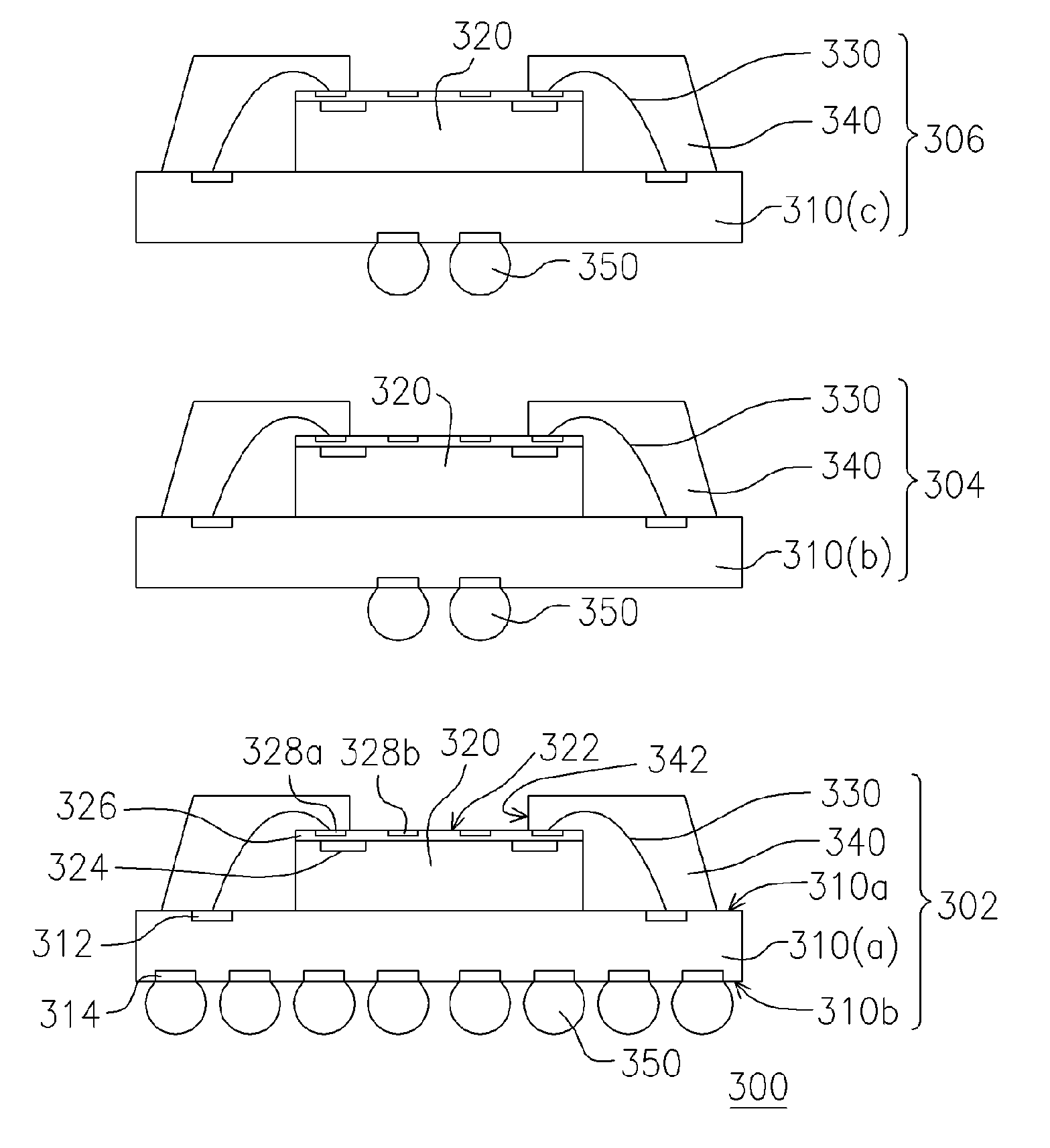
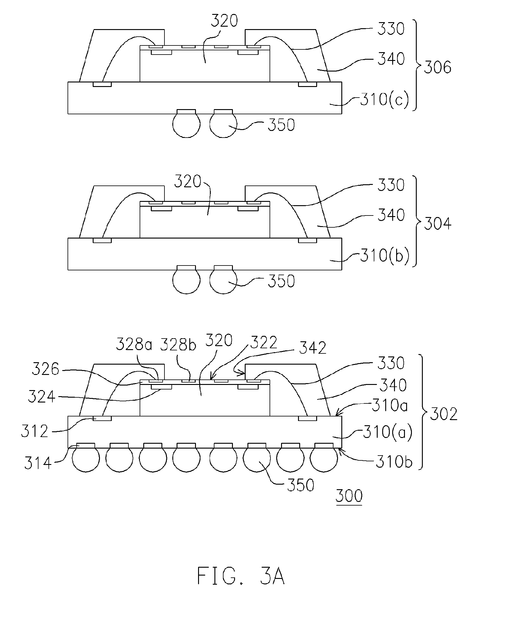
[0019]FIG. 3A is a disassembled view showing a stacked chip-packaging structure according to a preferred embodiment of the present invention. The stacked chip-packaging structure 300 consists essentially of a plurality of chip-packaging units 302, 304 and 306, each of which consists essentially of a substrate 310, a chip 320, a plurality of wires 330, a molding compound 340, and a plurality of solder balls 350. Wherein, the substrate 310 is made of, for example, ceramic, glass, or plastics. The substrate 310 has therein alternately stacked multiple conducting layers (not shown) and multiple insulating layers (not shown), while two adjacent conducting layers are separated by an insulating layer, and the conducting layers are electrically connected one another through conductive via or plating through hole. In addition, the top surface 310a and the bottom surface 310b of each of the substrates 310(a), (b) and (c), have respectively at least an upper contact 312 and a lower contact 314...


PUM


Abstract

A stacked chip-packaging structure consisting of a plurality of chip-packaging units is provided. Each of the chip-packaging units includes a substrate, a chip, a plurality of wires, a molding compound, and a plurality of solder balls. The chip-packaging units are, for example, of a BGA structure with high pin count, and are stacked up one over another and electrically connected through solder balls. With such structural features, the space that the stacked chip-packaging structure occupies is reduced and consequently the entire structure can be miniaturized.

Description

BACKGROUND OF THE INVENTION[0001]1. Field of the Invention[0002]The present invention relates to a chip-packaging structure, and more particularly to a stacked chip-packaging structure.[0003]2. Description of the Related Art[0004]With the progress of highly developed integrated circuit (IC) technologies, integration of internal circuits of IC chips steadily increases. As a result, number of transistors held in internal circuits of IC chips increases relatively, and sectional area of wires in the internal circuits of IC chips reduces accordingly. As the packaging technologies being continuously improved, various chip-packaging structures have been developed, including chip-packaging structures of ball grid array (BGA) structure and of multi-chip packaging module. Wherein, the BGA structure has advantages of high pin count and high reliability, while the multi-chip packaging module has shorter transfer route and better electronic properties. Such technical features make it possible to...

Claims


Application Information

Patent Timeline
Patent Type & Authority Patents(United States)
IPC IPC(8): H01L23/02H01L23/12H01L23/29H01L23/34H01L29/40H01L23/31H01L23/433H01L25/10
CPCH01L23/3128H01L24/73H01L25/105H01L23/4334H01L2225/1094H01L24/45H01L2224/45144H01L2224/48227H01L2224/73207H01L2224/8592H01L2924/01013H01L2924/0105H01L2924/01078H01L2924/01079H01L2924/01082H01L2924/09701H01L2924/14H01L2924/15311H01L2924/1815H01L2225/1058H01L24/48H01L2924/01005H01L2924/01006H01L2924/01033H01L2225/1088H01L2225/1023H01L2924/00014H01L2924/181H01L2924/00
Inventor TSAI, YU-FANGKANG, JUNG-KUNTSAI, TSUNG-YUEH
Owner ADVANCED SEMICON ENG INC
Why Eureka
Try Eureka