
Display device utilizing a plurality of adjoining display panels to form single display screen and methods related thereto

Inactive Publication Date: 2006-04-25
THE BOEING CO
View PDF24 Cites 2 Cited by
  • Summary
  • Abstract
  • Description
  • Claims
  • Application Information

AI Technical Summary

Benefits of technology

[0018]It is therefore an object of the present invention to provide a display device of a large screen formed by joining plural panels together which offers a natural image without generating light scattering at a connected part of the panels.
[0022]In the display device having the described arrangement, a space between adjoining display panels is filled with the bonding agent, and when joining the display panels together, a concentration of the internal stress caused by a curing shrinkage of the bonding agent is suppressed at the chamfered edge portion. Namely, at such edge portion, as a maximum value of the internal stress becomes smaller than an intermolecular bond strength of the bonding agent, a generation of cracks around the edge portion can be prevented. Therefore, as light scattering caused by such cracks can be reduced, a desirable display device of a large screen having an excellent visibility in which a joint of the display panels is not noticeable can be achieved.
[0024]According to the described arrangement, as the interval between the adjoining display panels is selected to be not more than 50 μm, the absolute value of the volumetric shrinkage due to the curing shrinkage of the bonding agent can be made smaller. This enables a value of the internal stress generated in the hardened bonding agent to be smaller than the intermolecular bond strength of the hardened bonding agent, thereby preventing a generation of cracks due to the hardened bonding agent around the edge portion. In the meantime, the internal stress is smaller than the bond strength between the bonding agent and the display panels, thereby preventing a generation of a peeling. As this prevents light scattering caused by cracks or a peeling at the connected part of the display panels, a desirable display device of a large screen having an excellent visibility in which a joint of the adjoining display panels is not noticeable can be achieved.
[0026]According to the described arrangement of the display device, even under the same curing shrinkage of the bonding agent, the internal stress generated by the curing shrinkage of the bonding agent is absorbed by the elasticity (flexibility) of the bonding agent. Namely, as the maximum value of the internal stress becomes smaller than the intermolecular bond strength of the hardened bonding agent, a generation of cracks due to the hardened bonding agent around the edge portion can be prevented. Furthermore, as the internal stress can be made smaller than the bond strength between the bonding agent and the display panels, a generation of peelings can be prevented. Namely, as light scattering due to cracks or peelings generated at the connected part of the display panels can be suppressed, a desirable display device of a large screen having an excellent visibility in which a joint of the display panels is not noticeable can be achieved.
[0028]According to the described arrangement of the display device, as the bonding agent can be more efficiently spread on the end surface portions of the display panels, generation of bubbles in a space between the end surface portions of the connected parts and the bonding agent can be prevented. Namely, the improved wettability permits display panels to be joined together without having residual bubbles remaining on the interface with the bonding agent, thereby preventing light scattering caused by such bubbles. As a result, a desirable display device of a large screen having an excellent visibility in which a joint of the display panels is not noticeable can be achieved.
[0030]In the display device of the described arrangement, the width of the connected part of the display panels can be reduced. Specifically, the width of the connected part of the display panels can be reduced to not more than 20 μm. Therefore, even under fluctuating index of refraction of the bonding agent, an adverse effect on color, or distortion of an image formed by light passing through the connected part of the display panels can be suppressed, thereby achieving a desirable display device of a large screen having an excellent visibility in which a joint of the display panels is not noticeable.

Problems solved by technology

However, the reduction in percent defective of each display element in the manufacturing process already faces the limit, and a significant progress is difficult to be expected.
Thus, it would be difficult to mass-produce the liquid crystal display device of a large screen which offers high quality images, and a cost for such liquid crystal display device remains too high.
Besides, if the end surface portion 52c becomes coarse in the manufacturing process, refraction and scattering of light would occur, thereby presenting the problem that the joint between the liquid crystal panels 52 stands out.
Such fine bubbles remaining in the space may again cause a scattering of light.

Method used


Image

  • Display device utilizing a plurality of adjoining display panels to form single display screen and methods related thereto
  • Display device utilizing a plurality of adjoining display panels to form single display screen and methods related thereto
  • Display device utilizing a plurality of adjoining display panels to form single display screen and methods related thereto

Examples


first embodiment

[0045]The following descriptions will discuss one embodiment of the present invention in reference to FIG. 1 through FIG. 4.

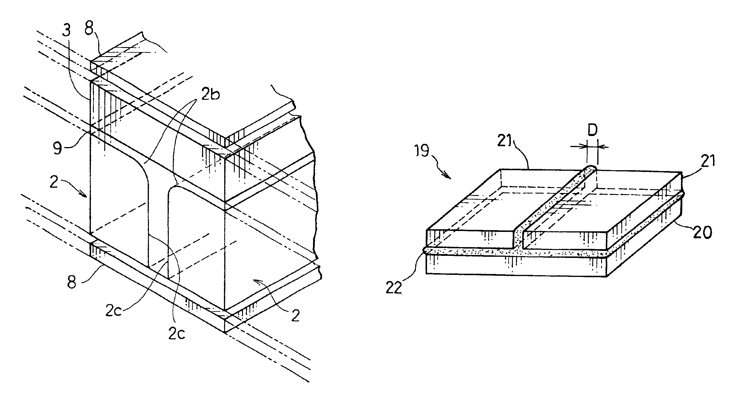
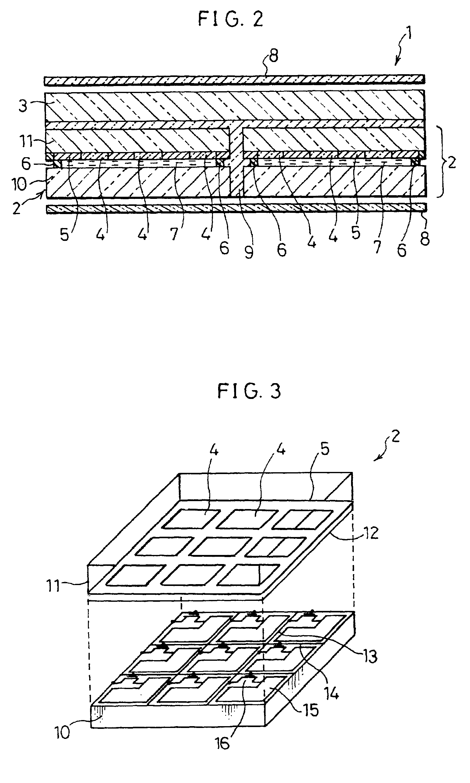
[0046]As shown in FIG. 2, a liquid crystal display device 1 in accordance with the present embodiment is of the direct sight type. The liquid crystal display device 1 includes liquid crystal panels 2 of an active matrix type provided on one surface of a reinforcing substrate 3 of an sufficient size to entirely cover the display screen of the liquid crystal display device 1. The liquid crystal display device 1 also includes polarization plates 8 (to be described later) which sandwich the reinforcing substrate 3 and the liquid crystal panels 2 in-between, a back light (not shown) such as a cold cathode gas discharge tube, for directing light onto the liquid crystal panels 2, and a driver (not shown) for driving the liquid crystal panels 2 based on the image information for displaying an image. The back light is provided on an opposite side to the reinforcing subs...

second embodiment

[0064]The following descriptions will discuss another embodiment of the present invention in reference to FIG. 5 through FIG. 8. For convenience in explanations, members having the same function as the aforementioned embodiment will be designated by the same reference numerals, and thus the descriptions thereof shall be omitted here.

[0065]FIG. 5(a) is a plan view showing a cutting position for a part to be connected in the process of bonding each liquid crystal panel 2. FIG. 5(b) is a plan view showing the state in which the liquid crystal panels 2 are joined together after their parts being cut. As shown in FIG. 5(a), one side of each liquid crystal panel 2 is cut along a cutting line 17 near an end of each image display area. Thereafter, the two liquid crystal panels 2 are bonded to the reinforcing substrate 3 in such a manner that the respective cut portions of the liquid crystal panels 2 are connected to each other.

[0066]As shown in FIG. 5(b), the liquid crystal panels 2 are typ...

third embodiment

[0081]The following descriptions will discuss still another embodiment of the present invention in reference to FIG. 9 and FIG. 10. For convenience in explanations, members having the same function as the aforementioned embodiment will be designated by the same reference numerals, and thus the descriptions thereof shall be omitted here.

[0082]It is described in the second embodiment that the width of the connected part of not more than 50 μm is sufficient for preventing generation of cracks, a peeling, etc., due to the curing shrinkage of the bonding agent 9. However, the index of refraction of the bonding agent 9 used in joining the liquid crystal panels 2 together varies depending on the composition, hardening conditions, or ambient temperature, etc. Therefore, in practice, it is difficult to adjust the index of refraction with accuracy of within the order of around 0.005 so that the index of refraction of the hardened bonding agent 9 is equal to that of the liquid crystal panel 2,...


PUM


Abstract

A display device of a multi-panel system is composed of plural liquid crystal panels which are jointed together by means of a bonding agent, and offers an image displayed on a large screen, wherein at least one edge portion of an end surface of a connected part of each liquid crystal panel is chamfered. According to the described arrangement, an internal stress generated by the curing shrinkage of the bonding agent at the chamfered portion is dispersed when joining the liquid crystal panels together, thereby preventing an occurrence of cracks at the edge portion. In this way, light scattering due to cracks at the joint between liquid crystal panels can be prevented. Accordingly, a liquid crystal display device of a large screen that offers excellent visibility in which a joint between liquid crystal panels does not stand out can be achieved.

Description

[0001]This application is a continuation of U.S. application Ser. No. 08 / 618,833, filed Mar. 20, 1996 (now allowed) U.S. Pat. No. 6,400,428, the teachings of which are incorporated herein by reference.FIELD OF THE INVENTION[0002]The present invention relates to a display device for use in AV (audio visual) equipments or OA (office automation) equipments.BACKGROUND OF THE INVENTION[0003]Recently, there has been an increasing demand for home TV sets representing AV equipments and display devices for use in OA equipments of improved characteristics such as light weight, thin structure, low power consumption, high definition performance and large screen, etc. To meet these demand, the development of display devices such as a CRT (cathode ray tube) display, an LCD (liquid crystal display), a PDP (plasma display panel), an EL (electro luminescent) display, and an LED (light emitting diode) display has been made to achieve improved characteristics thereof, and some of the display devices o...

Claims


Application Information

Patent Timeline
IPC IPC(8): G02F1/133G02F1/13G02F1/1333G02F1/1347
CPCG02F1/13336G02F1/13
Inventor IZUMI, YOSHIHIRO
Owner THE BOEING CO
Learn More