Optical modulator, display device and manufacturing method for same

a technology of optical modulators and display devices, applied in the field of optical modulators, can solve the problems of high manufacturing costs and significant manufacturing time, and achieve the effect of improving color reproduction quality and forming precision

Inactive Publication Date: 2006-04-25
SEIKO EPSON CORP
View PDF14 Cites 160 Cited by
  • Summary
  • Abstract
  • Description
  • Claims
  • Application Information

AI Technical Summary

Benefits of technology

[0032]forming a recess section or groove section by patterning a transparent substrate in accordance with the disposition of the movable reflective film in the first substrate; forming a transparent electrode film inside the recess section or groove section of the transparent electrode; and forming an absorbing film for absorbing incident light under prescribed conditions, on the transparent electrod

Problems solved by technology

However, the manufacturing process for an interference optical modulator is a complicated one comprising repeated deposition of films having different functions, f

Method used


Image

  • Optical modulator, display device and manufacturing method for same
  • Optical modulator, display device and manufacturing method for same
  • Optical modulator, display device and manufacturing method for same

Examples


Embodiment Construction

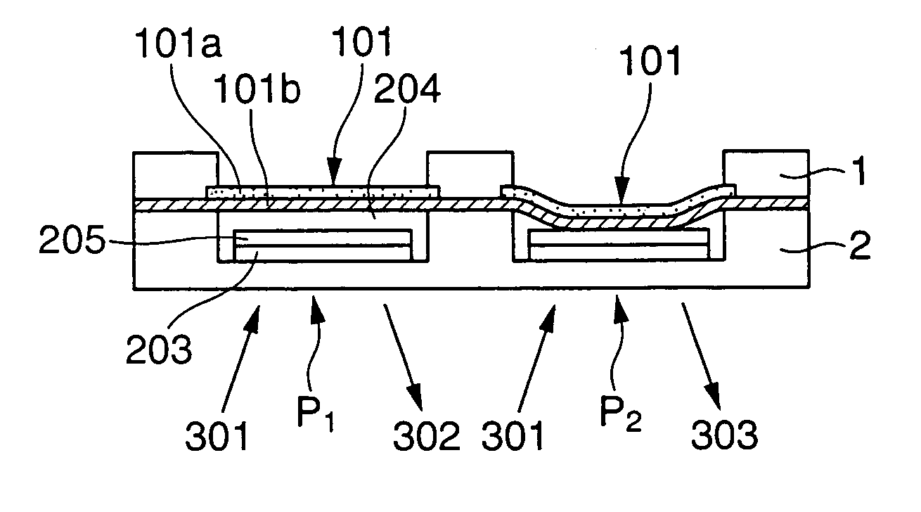
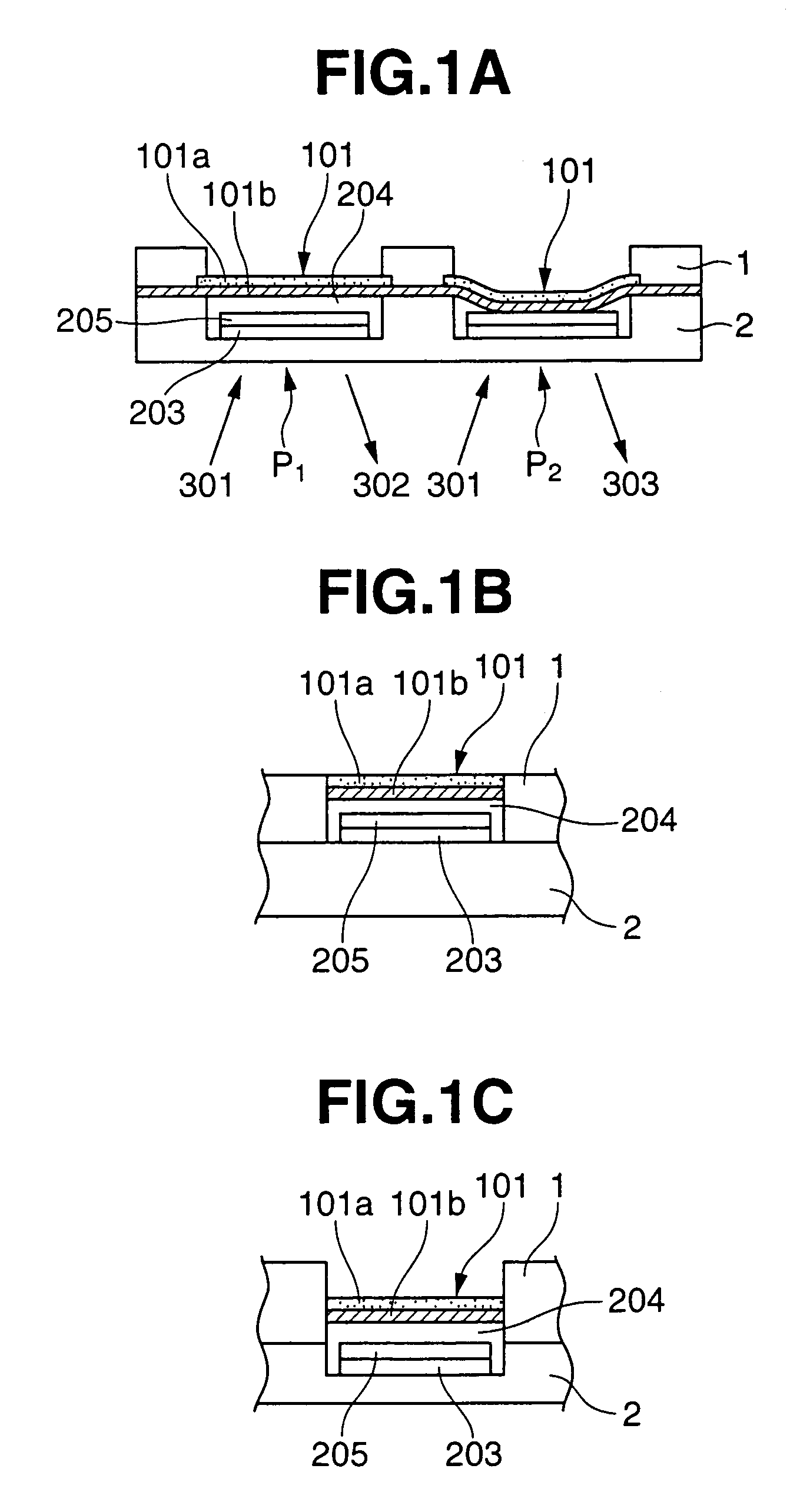
[0042]FIG. 1 is an illustrative diagram for describing an optical modulator according to an embodiment of the present invention, FIG. 1A is a cross-sectional diagram for describing the structure and the operational mechanism of an optical modulator according to the present embodiment, and FIGS. 1B and C are cross-sectional diagrams for illustrating a further embodiment of the optical modulator.

[0043]Firstly, the structure and operational mechanism of the optical modulator according to the present embodiment are described with respect to FIG. 1A.

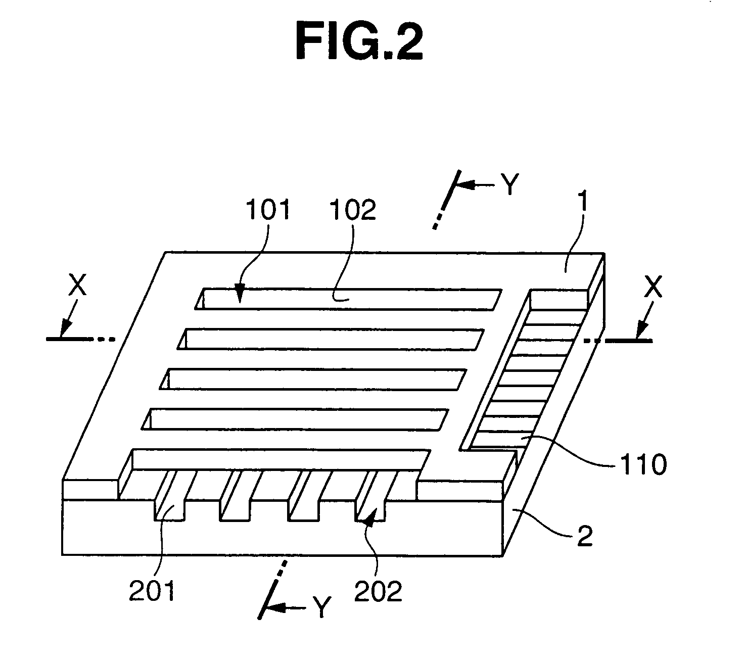
[0044]As shown in this diagram, the optical modulator is formed by joining a first substrate 1 and a second substrate 2, and comprises a cavity section 204 demarcated by the first substrate 1 and the second substrate 2. A transparent electrode 203 and a light absorber 205 are formed inside this cavity section 204.

[0045]The first substrate 1 is formed, for example, by a semiconductor substrate, and more specifically, by an N-type silicon subst...


PUM

PropertyMeasurementUnit
Timeaaaaaaaaaa
Polarityaaaaaaaaaa
Transparencyaaaaaaaaaa

Abstract

An optical modulator is provided which can be manufactured by means of a simple process, and a display device, and a method of manufacturing same. The optical modulator comprises a first substrate having a movable reflective film that oscillates in accordance with the application of an electrostatic force; a light-transmitting second substrate disposed so as to oppose the first substrate and formed with a transparent electrode for applying the electrostatic force, in a position corresponding to the movable reflective film; and a cavity section, demarcated by the first substrate and the second substrate, for restricting the range of oscillation of the movable reflective film. By forming a movable reflective film by a portion of the substrate and determining the range of oscillation of the movable reflective film by the interval between the substrates, an optical modulator of high durability and high precision can be obtained.

Description

RELATED APPLICATIONS[0001]The present application claims priority to Japanese Patent Application No. 2003-008766 filed Jan. 16, 2003 which is hereby expressly incorporated by reference in its entirety.BACKGROUND OF THE INVENTION[0002]1. Field of the Invention[0003]The present invention relates to an optical modulator which can be used for displaying still images, moving images and displays of other kinds, and more particularly, to improvements in an optical modulator and display device using an interference optical modulation, and to a method of manufacturing same.[0004]2. Description of the Related Art[0005]An optical modulator generates desired intensity and colouring, and the like, in transmitted light, by changing the optical parameters, such as the transmittance, refractive index, reflectivity, polarisation rate, interference, and the like, of light in an optical system.[0006]For example, an optical modulator based on light interference uses a reflective film whose position alt...

Claims


Application Information

Patent Timeline
IPC IPC(8): G02B26/00B81B3/00B81C1/00G02B26/08
CPCG02B26/0825G02B26/001
Inventor MAKIGAKI, TOMOHIRO
Owner SEIKO EPSON CORP
Why Eureka
Try Eureka