Drive unit for optical switch

a technology of drive circuit and optical switch, which is applied in the direction of optics, optical elements, instruments, etc., can solve the problems of unacceptable consumption power of the entire optical switch including the drive circuit, and no suggestion about the configuration of the drive circuit for applying voltage to the electrode, so as to achieve the effect of reducing the size of the hardware configuration and effectively reducing the consumption power

Inactive Publication Date: 2006-04-25
FUJITSU LTD
View PDF7 Cites 0 Cited by
  • Summary
  • Abstract
  • Description
  • Claims
  • Application Information

AI Technical Summary

Benefits of technology

[0021]With the drive unit described above, a plurality of micro-mirrors can be simultaneously controlled by a single drive circuit. Therefore, the scale of a hardware configuration can be greatly reduced and consumption power can be effectively reduced.

Problems solved by technology

However, no suggestions have been made about a configuration of a drive circuit part for applying voltages to electrodes.
Therefore, an overall size and consumption power of the entire optical switch including the drive circuit becomes unacceptably large.

Method used


Image

  • Drive unit for optical switch
  • Drive unit for optical switch
  • Drive unit for optical switch

Examples


second embodiment

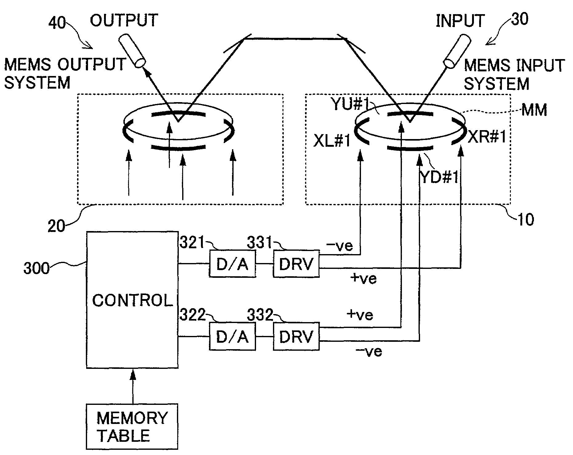
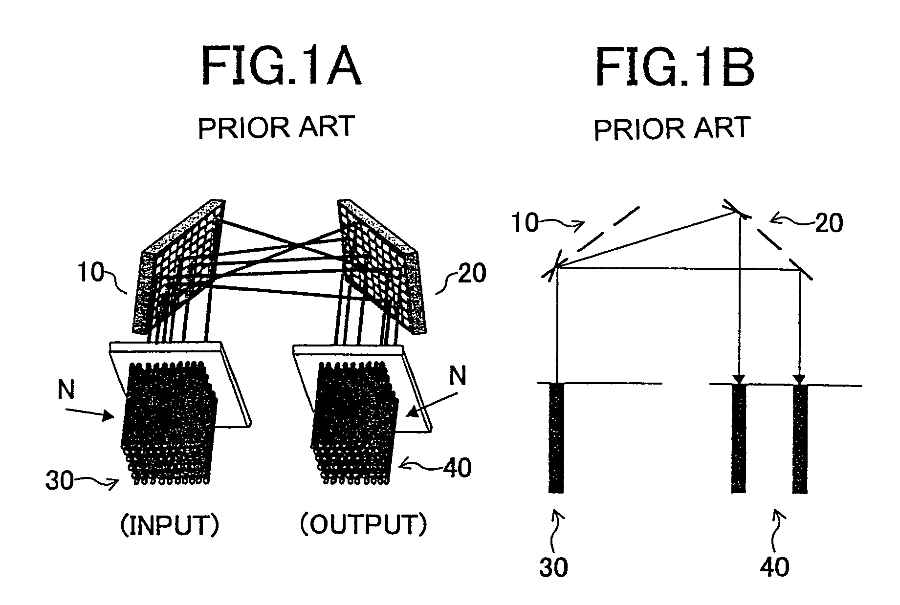
[0061]In the present invention, the drive unit is further provided with offset adjustment circuits 341, 342 connected to the drive circuits 331 and 332. It is to be noted that the circuit structure shown in FIG. 7 already incorporated the offset adjustment circuit. Considering a symmetric property of the mirror disposition shown in FIGS. 1A and 1B, it is preferable that maximum tilt angles for on the left side and the right side (or on the upper side and the lower side) of an axis are the same for each micro-mirror MM. To this end, it suffices with a situation where a positive voltage peak value and a negative voltage peak value are equal after separating the positive voltage and the negative voltage. This can be achieved by a circuit for adjusting output offsets.

[0062]That is to say, as shown in FIG. 11A, when the output voltages before separation into positive and negative voltages (i.e., the voltage at connection point P between the diodes D3 and D4) is not symmetrical for the po...

third embodiment

[0064]A drive unit of the present invention will be described with reference to FIGS. 12 and 13.

[0065]In the present embodiment, the drive unit is further provided with gain-adjusting circuits 351 and 352 connected to the drive circuits 331 and 332. It is to be noted that the circuit structure shown in FIG. 7 already incorporated the offset adjustment circuit. The gain adjustment circuits 351 and 352 may be added to an embodiment of the drive unit shown inFIG. 10.

[0066]As shown in FIG. 13, the voltage (V) for achieving a required tilt angle (θ) of the micro-mirror MM (V-θ characteristics) can be uniquely derived. The control circuit 400 has a memory table whereon the V-θ characteristics of the micro-mirror MM is prestored. The circuit 400 reads out voltage information corresponding to the required tilt angle of the micro-mirror MM from the memory table and outputs the voltage information in the form of digital signals. The D / A converters 312 and 322 convert the digital signals into ...

fourth embodiment

[0068]A drive unit of the present invention will be described with reference to FIG. 14.


PUM

PropertyMeasurementUnit
voltageaaaaaaaaaa
voltageaaaaaaaaaa
voltageaaaaaaaaaa

Abstract

A drive unit for controlling optical paths of an optical switch having at least one optical switch element and at least one pair of electrodes arranged near the optical switch element, each pair including a first electrode and a second electrode provided at a position opposite to the first electrode. The drive unit includes at least one drive circuit for the at least one optical switch element, respectively. The drive circuit has an output for supplying voltages to the electrodes to generate electrostatic forces between the electrodes and the optical switch element and the voltages are separated into positive voltages supplied to the first electrode and negative voltages supplied to the second electrode.

Description

BACKGROUND OF THE INVENTION[0001]1. Field of the Invention[0002]The present invention relates to a drive unit for an optical switch and particularly relates to a drive unit for an optical switch that can be applied in an optical network.[0003]Recently, amount of data traffics transmitted on networks is sharply increasing due to rapid growth of the Internet. Therefore, a network configuration needs to be changed from a ring-type configuration to a mesh-type configuration to establish and release communication paths in a more dynamic manner. To this end, a large-scale cross-connect (XC) apparatus is required. However, currently available XC apparatuses do not have sufficient capacity (data capacity) and have limitations on electric signal processing for increased signal bit-rate. Therefore, it is difficult to build a large-scale optical switch system with currently available XC apparatuses.[0004]MEMS (Micro-Electro Mechanical System) is one of the technologies that may be applied to s...

Claims


Application Information

Patent Timeline
Patent Type & Authority Patents(United States)
IPC IPC(8): G02B6/35H04Q11/00G02B26/08
CPCH04Q11/0005G02B6/357G02B6/3512G02B6/3546G02B6/3556H04Q2011/0039H04Q2011/003
Inventor YAMASHITA, SHINJIMORI, KAZUYUKI
Owner FUJITSU LTD
Why Eureka
Try Eureka