Semiconductor devices and manufacturing method therefor and electronic commerce method and transponder reader

a semiconductor device and manufacturing method technology, applied in the direction of instruments, resonant antennas, burglar alarm mechanical actuation, etc., can solve the problems of reduced connection area, increased resistance, unstable operation of wireless ic chips, etc., to improve the speed of successive readings, improve accuracy, and improve economic efficiency. effect of placing orders

Inactive Publication Date: 2006-05-02
HITACHI LTD
View PDF17 Cites 35 Cited by
  • Summary
  • Abstract
  • Description
  • Claims
  • Application Information

AI Technical Summary

Benefits of technology

[0062]Also, according to the electronic commerce method of items (12) and (24), by establishing the link to the server of the supplier of the product via wireless, it is possible to improve the speediness, the accuracy, and the econom

Problems solved by technology

First, in the wireless IC tag, the following problems occurs because a plurality of electrodes have to be placed on one surface (front surface) of the wireless IC chip.
Firstly, the smaller the chip size of the wireless IC chip is, the smaller the size of the electrode becomes, thereby causing the size reduction of a connection area.
Consequently, the

Method used


Image

  • Semiconductor devices and manufacturing method therefor and electronic commerce method and transponder reader
  • Semiconductor devices and manufacturing method therefor and electronic commerce method and transponder reader
  • Semiconductor devices and manufacturing method therefor and electronic commerce method and transponder reader

Examples


first embodiment

[0116](First Embodiment)

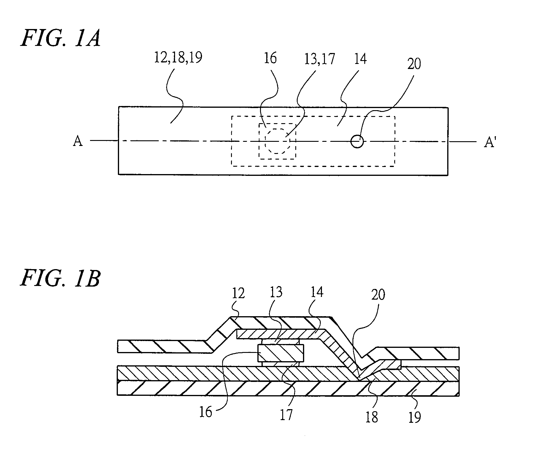
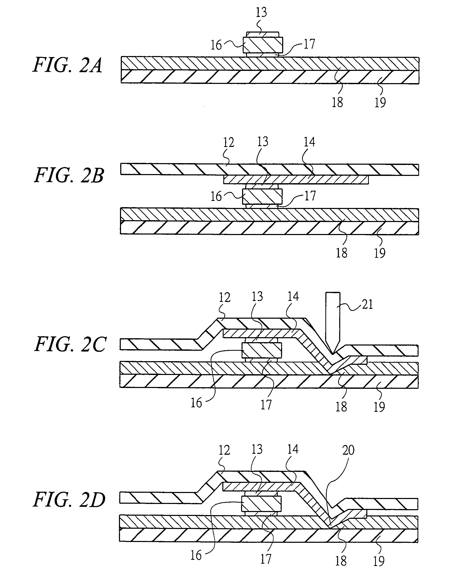
[0117]FIGS. 1A and 1B are diagrams showing a structure of a semiconductor device according to a first embodiment of the present invention, wherein FIG. 1A is a plan view and FIG. 1B is a cross-sectional view taken along the line A–A′ in FIG. 1A.

[0118]First, an example of the structure of the semiconductor device according to the first embodiment will be described with reference to FIG. 1. The semiconductor device according to this embodiment is, for example, an IC tag, which comprises an upper substrate 12, an upper electrode (bump or the like) 13, a first conductor (metal or the like) 14, a wireless IC chip 16, a lower electrode (bump or the like) 17, a second conductor (metal or the like) 18, and a lower substrate 19, etc.

[0119]The first conductor 14 adheres to the upper substrate 12, and the second conductor 18 adheres to the lower substrate 19. The wireless IC chip 16, having the upper electrode 13 and the lower electrode 17, is sandwiched between the fir...

second embodiment

[0133](Second Embodiment)

[0134]FIGS. 3 to 6 are plan views showing a structure of a semiconductor device according to a second embodiment of the present invention.

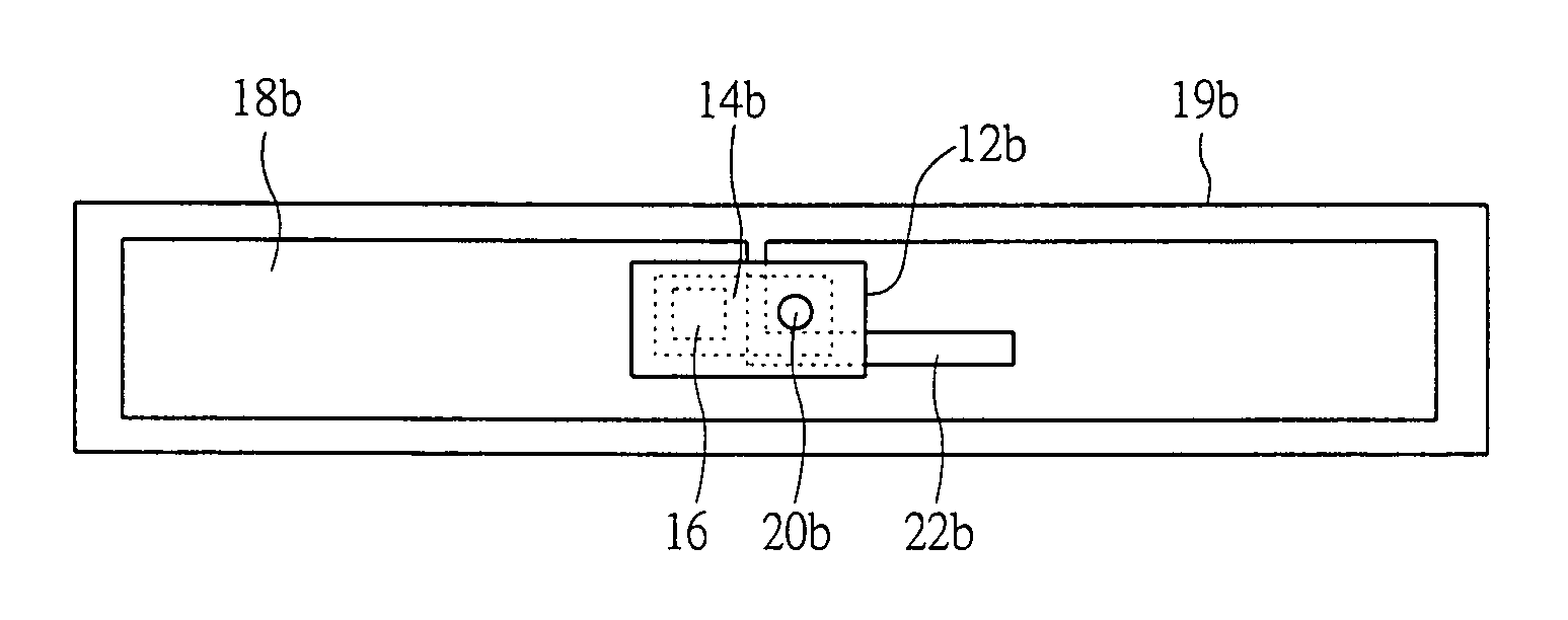
[0135]First, an example of the structure of the semiconductor device according to the second embodiment will be described with reference to FIG. 3. The semiconductor device according to the second embodiment is, for example, an IC tag, which includes an upper substrate 12a, an upper electrode (not shown), a first conductor 14a, a wireless IC chip 16, a lower electrode (not shown), a second conductor 18a, and a lower substrate 19a, etc.

[0136]The first conductor 14a adheres to the upper substrate 12a, and the second conductor 18a adheres to the lower substrate 19a. The wireless IC chip 16 with the upper electrode and the lower electrode is sandwiched between the first conductor 14a and the second conductor 18a. The first conductor 14a and the second conductor 18a are electrically connected via a conductor-connection portion ...

third embodiment

[0151](Third Embodiment)

[0152]FIGS. 8A and 8B are plan views showing a structure of a semiconductor device according to a third embodiment of the present invention. FIG. 8A shows the state before the fabrication, and FIG. 8B shows the state after the fabrication. FIG. 9 is a cross-sectional view taken along the line B–B′ in FIG. 8B.

[0153]First, an example of the structure of the semiconductor device according to the third embodiment will be described with reference to FIGS. 8 and 9. The semiconductor device according to the third embodiment is, for example, an IC tag, which includes a substrate 12e, an upper electrode (not shown), a first conductor portion 14e, a wireless IC chip 16, a lower electrode (not shown), and a second conductor portion 18e, etc.

[0154]The conductor adheres to the substrate 12e. The wireless IC chip 16 with the upper electrode and the lower electrode is sandwiched between the first conductor portion 14e and the second conductor portion 18e (see FIGS. 8B and 9...


PUM


Abstract

In a wireless IC tag utilizing a wireless IC chip, the wireless IC tag having sufficient stress strength is manufactured economically. There is adopted a structure in which an upper electrode and a lower electrode are respectively formed on a front surface and a rear surface of a wireless IC chip, and the upper electrode is connected to a first conductor and a lower electrode is connected to a second conductor, and the first conductor and the second conductor are connected outside the wireless IC chip. Thereby, it is possible to fabricate the wireless IC tag economically and to ensure the stress strength.

Description

BACKGROUND OF THE INVENTION[0001]The present invention relates to a semiconductor device, a manufacturing method for the semiconductor device, an electronic commerce method, and a transponder reader, and more particularly to a technique effectively applied to a structure of a wireless IC chip used to identify an object in a non-contact manner, an IC tag for wirelessly sending an identification number, a transponder, or the like.[0002]For example, the following techniques can be taken as techniques examined by the inventors of the present invention with respect to a wireless IC tag employing a wireless IC chip and / or to a transponder reader etc.[0003]For example, the wireless IC tag is fabricated with the structure as shown in FIG. 29. The structure is not the technique of the wireless IC tag but is obtained by applying the technique (see, for example, Patent Document 1) used in the manufacturing method for a semiconductor device such as a transistor. A plurality of electrodes (bumps...

Claims


Application Information

Patent Timeline
IPC IPC(8): G06K19/06H01L21/60G06K17/00G06K19/00G06K19/07G06K19/077G06Q10/00G06Q30/06G06Q50/00G06Q50/04H01Q13/08H01Q13/10
CPCG06K19/07728G06K19/07745G06K19/07749G06K19/0775H01L2924/07811H01L2224/16227H01L2924/13091H01L2224/16225H01L2924/00H01L21/60
Inventor USAMI, MITSUOSATO, AKIRA
Owner HITACHI LTD
Why Eureka
Try Eureka