

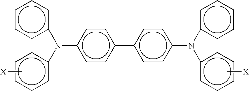
Photoconductive members
a photoconductive and member technology, applied in the field of photoconductive members, can solve the problems of multi-layered imaging members, high cost and time consumption, and the inability of thin photogenerating layer to fully absorb imaging laser light, and achieve the effect of optimum performance and cos
- Summary
- Abstract
- Description
- Claims
- Application Information
AI Technical Summary
Benefits of technology
Problems solved by technology
Method used
Image


Examples
example ii
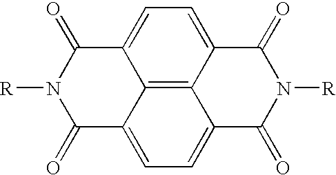
[0065]Another series of single layer photoresponsive imaging members were fabricated in accordance with Example I except that the NTDI was replaced by the electron transport molecule (4-n-butoxycarbonyl-9-fluorenylidene)malononitrile, BCFM. The xerographic evaluation was performed for these members and results are summarized in Table C.
[0066]
TABLE CXerographic Electricals of Single Layer PhotoresponsiveMembers with BCFMImagingWeight Ratio ofDarkE1 / 2Member IDHOGaPc:x-H2PcDecay V / sErg / cm22A100:0 841.322B75:25781.572C50:50771.772D25:75751.952E 0:100842.12
[0067]Though the replacement of NTDI by BCFM led to higher dark decay than in those of Table B, the variation of photosensitivity shows an excellent linear dependence on the pigment composition. A regression plot of E1 / 2 versus pigment composition gives R2=0.9849.
example iii
[0074]The xerographic electricals of photoresponsive members in Example I were also evaluated under negatively charging conditions. The measuring conditions were identical to those described in Example I except that the corona device was now negatively charged. The xerographic evaluation results are summarized in Table F.
[0075]
TABLE FXerographic Electricals of Single Layer Photoresponsive MembersUnder Negative Corona ChargingImagingWeight Ratio ofDarkE1 / 2Member IDHOGaPc:x-H2PcDecay V / sErg / cm21A100:0 364.241B75:25496.021C50:50549.471D25:756113.71E 0:1006617
[0076]The single layer photoreceptors of this invention can also function under negative charging conditions, and hence they are bipolar. However, the photosensitivities under negative charging conditions were relatively lower than those measured under positive charging shown in Example I. A regression plot of E1 / 2 versus pigment composition gives R2=0.9846 indicating that the variation of photosensitivity shows a linear dependence...
PUM
 Abstract
Description
Claims
Application Information