Stabilization of dopant concentration in semiconductor device having epitaxially-filled trench

a technology of epitaxial filling and stabilizing dopant concentration, which is applied in the direction of semiconductor devices, basic electric elements, electrical equipment, etc., can solve the problems of fluctuation and deviation of dopant concentration in the substra

Inactive Publication Date: 2006-05-02
DENSO CORP
View PDF14 Cites 11 Cited by
  • Summary
  • Abstract
  • Description
  • Claims
  • Application Information

AI Technical Summary

Problems solved by technology

However, there is a problem in the method of U.S. Pat. No. 6,406,982 that the dopant concentration in the substrate 132 can fluctuate to deviate from the predetermined concentration because the dopants contained in the semiconductor substrate 132 out diffuse during the heating.

Method used


Image

  • Stabilization of dopant concentration in semiconductor device having epitaxially-filled trench
  • Stabilization of dopant concentration in semiconductor device having epitaxially-filled trench
  • Stabilization of dopant concentration in semiconductor device having epitaxially-filled trench

Examples


first embodiment

[0020

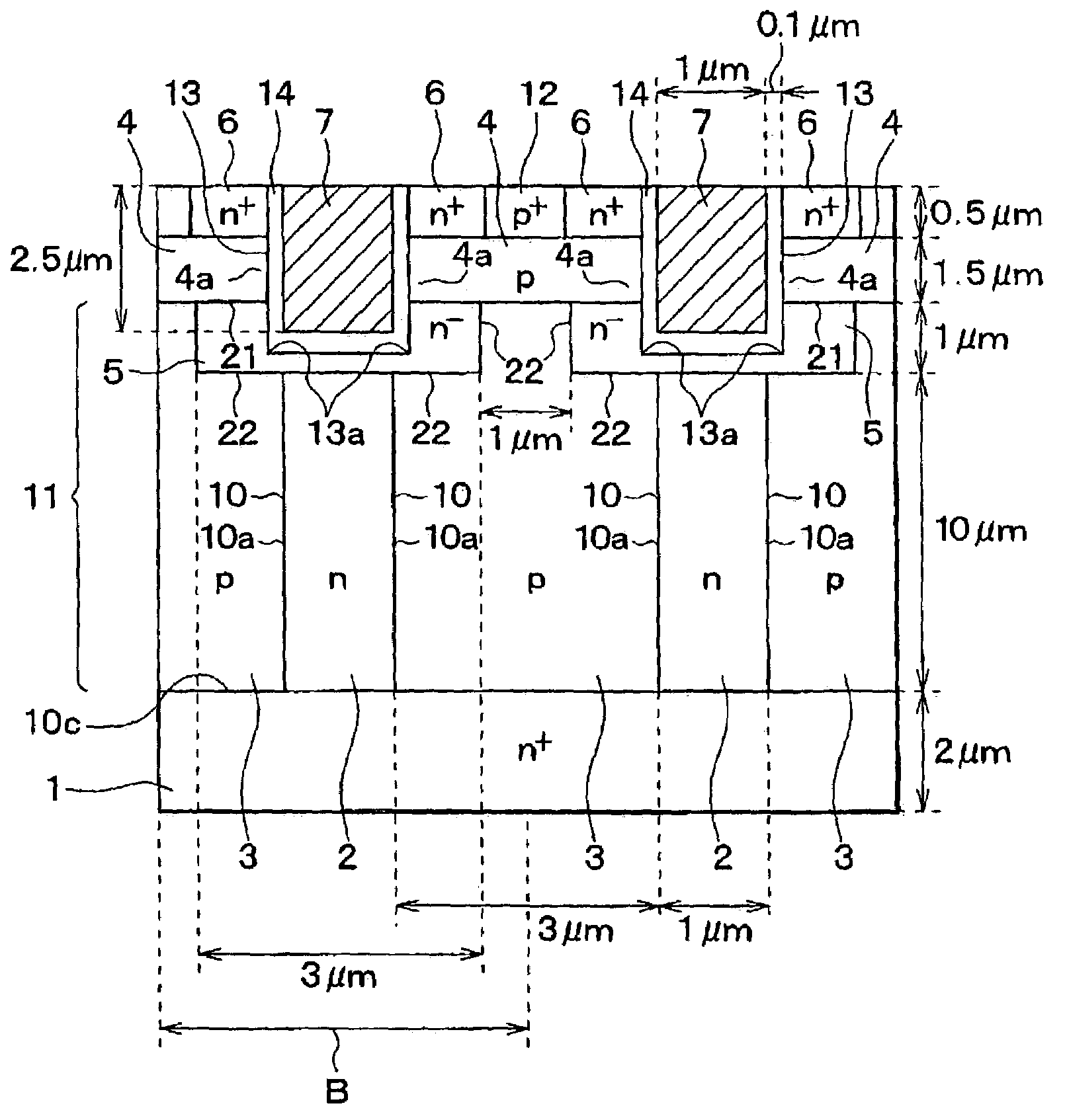
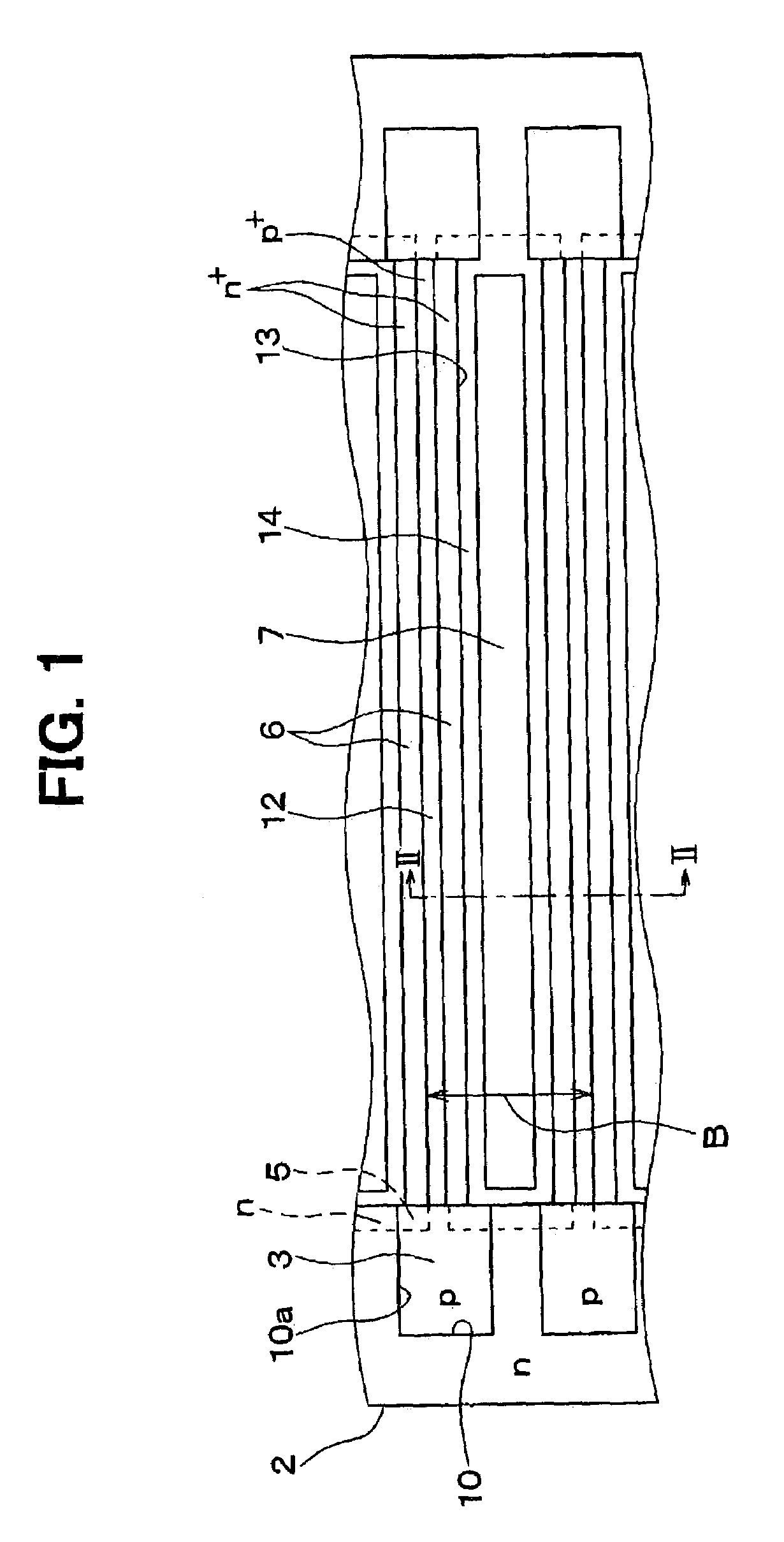
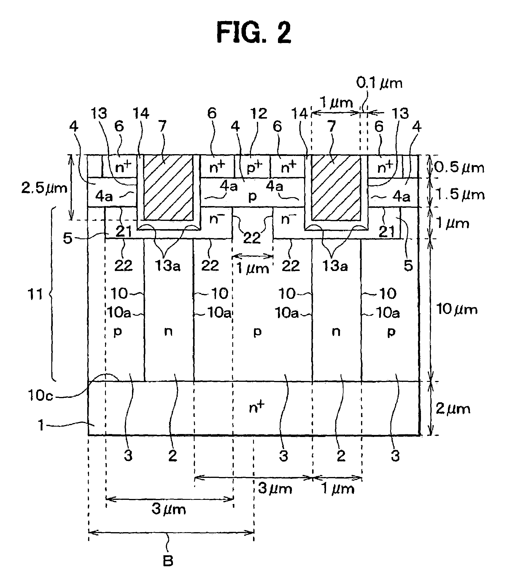
[0021]FIG. 1 is a plan view of a power MOSFET having a super junction structure according to a first embodiment of the present invention. FIG. 2 is a cross-sectional view of the power MOSFET taken along the line II—II in FIG. 1. In this power MOSFET, a structure within a range having a width B is a single unit structure, which is repeated a plurality of times to form this power MOSFET. This power MOSFET includes an n+-type substrate 1, n-type drift regions 2, p-type silicon regions 3 as first semiconductor regions 3, p-type base regions 4, upper n-type silicon regions 5 as second semiconductor regions 5, n+-type source regions 6, and gate electrodes 7.

[0022]The n+-type substrate 1 forms an n+-type drain region 1, and the thickness of the n+-type substrate 1 is, for example, 2 μm in a vertical direction of the n+-type substrate 1. The substrate 1 has a dopant concentration of 1×10¹⁹ to 1×1023 cm−3. The n-type drift regions 2 are located on the n+-type substrate 1 and have, for e...

second embodiment

[0069

[0070]FIG. 5 is a partial schematic plan view of a power MOSFET having a super junction structure according to a second embodiment. FIG. 6 is a schematic cross-sectional view of the device in FIG. 5 taken along the line VI—VI. The cross-sectional structure of the device of FIG. 5 taken along the line II—II in FIG. 5 is the same as that shown in FIG. 2, and the portion that has the cross-sectional structure along the line II—II in FIG. 5 is a unit element. The cross-sectional view, which is shown in FIG. 6, of the device of FIG. 5 taken along the line VI—VI in FIG. 5 shows an end of the power MOSFET of FIG. 5.

[0071]The power MOSFET according to this embodiment has the structure in which a low dopant concentration region 41 is added to the power MOSFET shown in FIG. 1 around the super junction such that the low dopant concentration region 41 has a dopant concentration lower than the regions that make up the super junction. There are no differences in other aspects. Therefore, the...


PUM


Abstract

A method for manufacturing a semiconductor device includes: forming a trench in a predetermined layer of a semiconductor substrate; heating the substrate having the trench in a non-oxidizing and non-nitridizing atmosphere containing a dopant or a compound that includes the dopant in order to smooth the surfaces defining the trench and to maintain the dopant concentration in the predetermined layer to be a predetermined concentration before the heating is treated; and forming an epitaxially grown film to fill the trench. The conductivity type of the dopant contained in the non-oxidizing and non-nitridizing atmosphere is the same as that of the dopant initially contained in the predetermined layer.

Description

CROSS REFERENCE TO RELATED APPLICATION[0001]This application is based on and incorporates herein by reference Japanese Patent Application No. 2002-161594 filed on Jun. 3, 2002.BACKGROUND OF THE INVENTION[0002]The present invention relates to a semiconductor device, in the manufacturing process of which a trench is filled with an epitaxially grown film, and a method for manufacturing the device.[0003]The inventors of the present invention propose the following method, which is shown in FIGS. 8A to 8F, for forming a trench in a semiconductor layer and filling the trench with an epitaxially grown film in U.S. Pat. No. 6,406,982 (JP-A-2002-124474). In the method, firstly, an n-type drift layer 120 is formed on an n+-type substrate 110 to form a semiconductor substrate 132, and a mask layer 131 is formed by patterning a film deposited on the substrate 132 using photolithography and etching, as shown in FIG. 8A.[0004]Then, the n-type drift layer 120 is partially etched using the mask laye...

Claims


Application Information

Patent Timeline
Patent Type & Authority Patents(United States)
IPC IPC(8): H01L21/76H01L21/205H01L21/20H01L21/324H01L21/336H01L29/06H01L29/78
CPCH01L29/7813H01L29/0634H01L21/02381H01L21/02532H01L21/02658H01L21/02573
Inventor YAMAUCHI, SHOICHIYAMAGUCHI, HITOSHI
Owner DENSO CORP
Why Eureka
Try Eureka