Methods of forming planarized surfaces over semiconductor substrates

a technology of semiconductor substrates and planarized surfaces, which is applied in the direction of semiconductor/solid-state device manufacturing, basic electric elements, electric devices, etc., can solve the problems of affecting the rate of material removal by cmp, difficult to control the cmp process within tight tolerances, and difficult to ascertain an appropriate stop point within the material, etc., to achieve better uniformity and improve post-cmp thickness uniformity

Active Publication Date: 2006-05-02
MICRON TECH INC
View PDF18 Cites 47 Cited by
  • Summary
  • Abstract
  • Description
  • Claims
  • Application Information

AI Technical Summary

Problems solved by technology

A problem with planarization of a single material is that it is difficult to ascertain an appropriate stop point within the material.
However, minor variations in temperature, type of slurry, polishing pad wear, etc. can impact the rate of removal of material by CMP.
This can make it difficult to control CMP processes within the tight tolerances desired for modern semiconductor device processing.
If the CMP process is not appropriately maintained within desired tolerances, there can be a non-uniform thickness of material across the substrate after the CMP, which can create difficulties in fabrication steps following the CMP.

Method used


Image

  • Methods of forming planarized surfaces over semiconductor substrates
  • Methods of forming planarized surfaces over semiconductor substrates
  • Methods of forming planarized surfaces over semiconductor substrates

Examples


Embodiment Construction

[0016]This disclosure of the invention is submitted in furtherance of the constitutional purposes of the U.S. Patent Laws “to promote the progress of science and useful arts” (Article 1, Section 8).

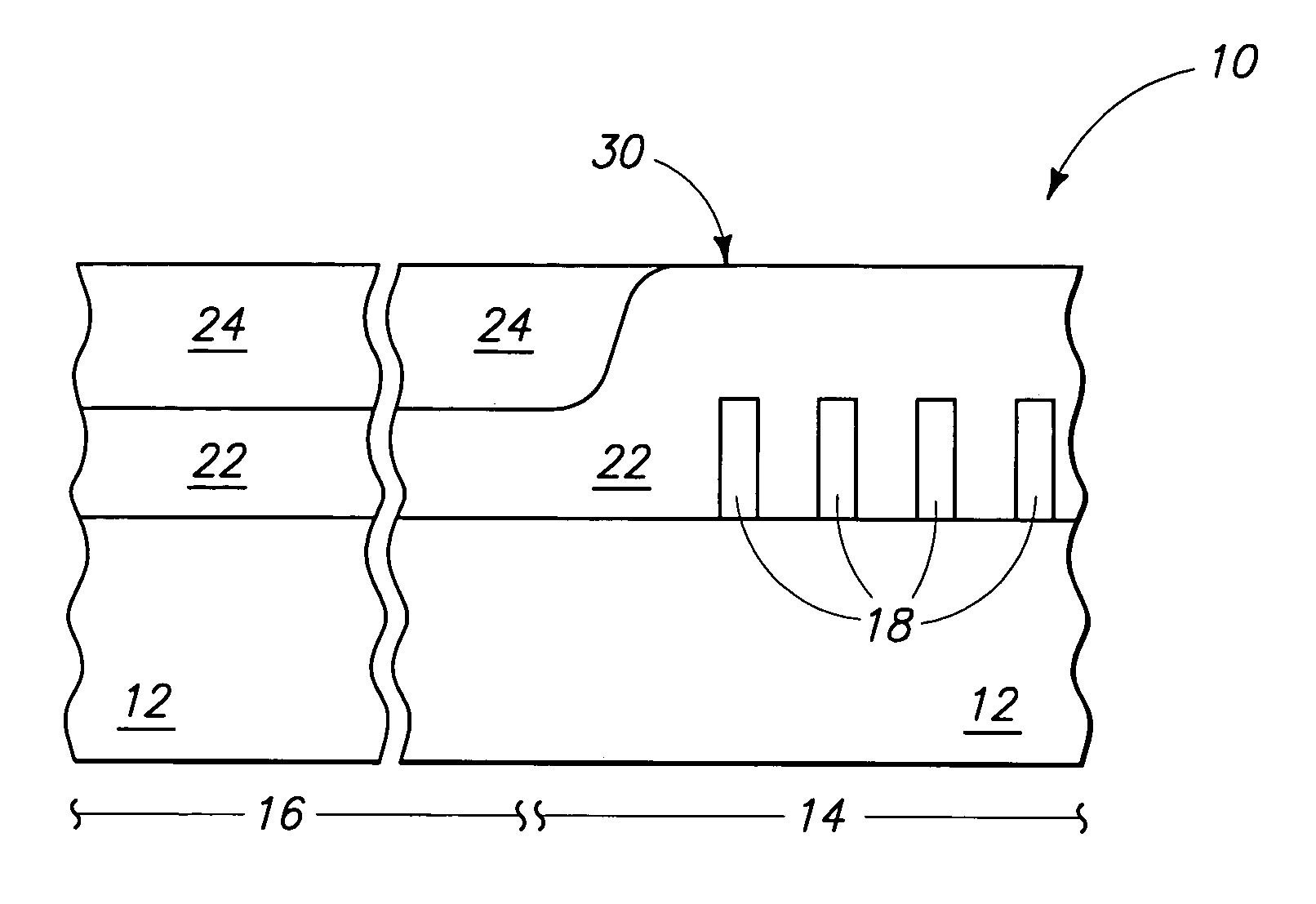
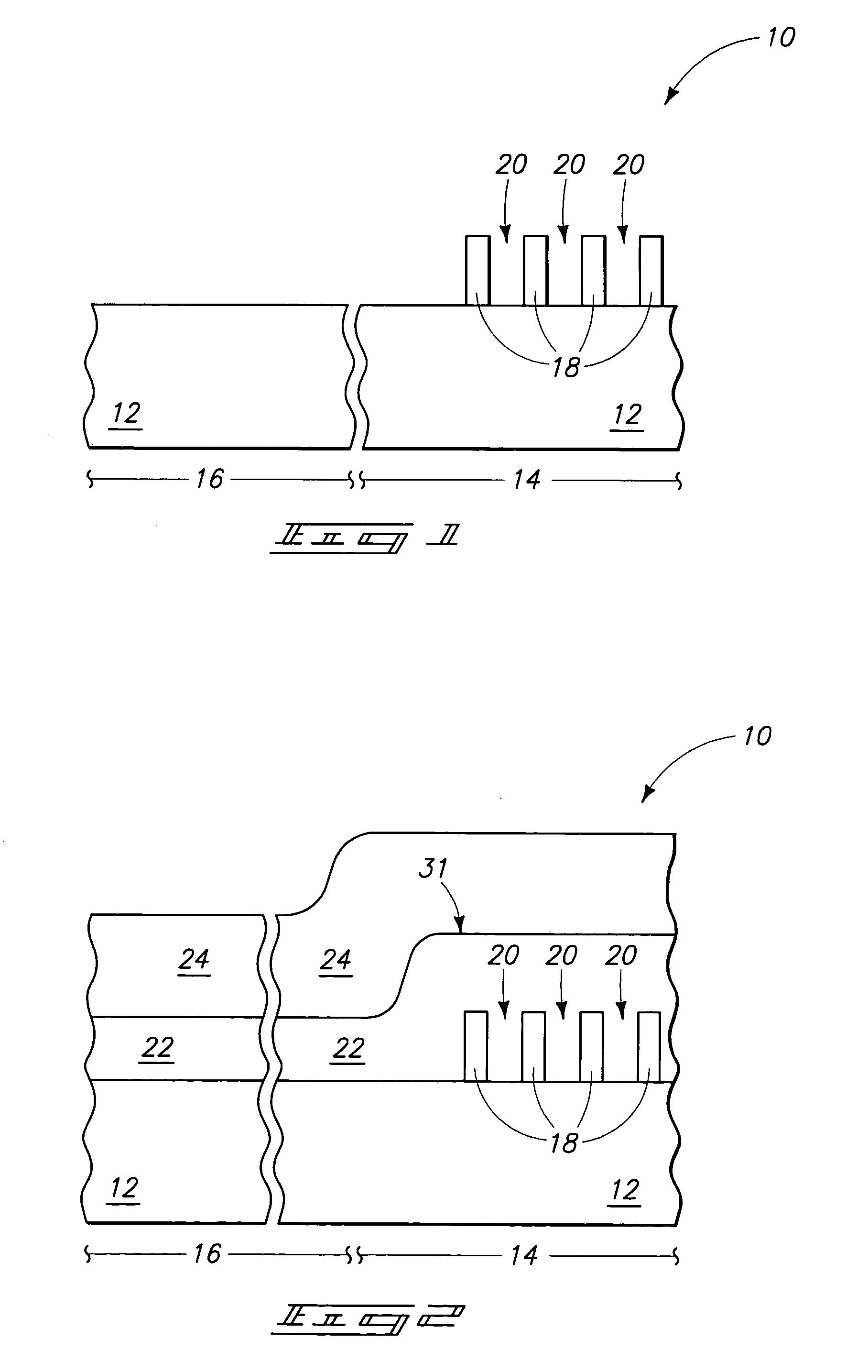
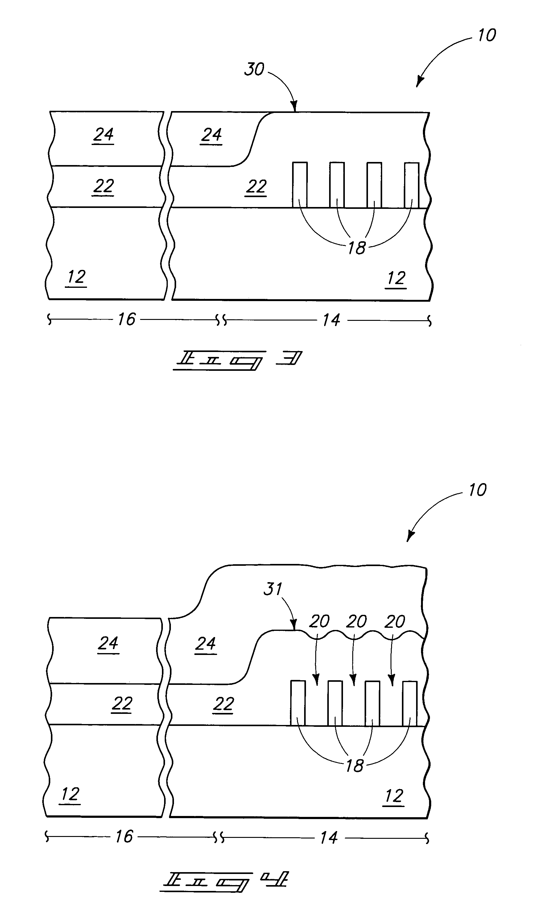
[0017]An exemplary aspect of the invention is described with reference to FIGS. 1–3. Referring initially to FIG. 1, a fragment 10 of a semiconductor wafer is illustrated at a preliminary processing stage. Fragment 10 comprises a base 12 which can comprise, consist essentially of, or consist of monocrystalline silicon lightly-doped with background p-type dopant.

[0018]To aid in interpretation of the claims that follow, the terms “semiconductive substrate” and “semiconductor substrate” are defined to mean any construction comprising semiconductive material, including, but not limited to, bulk semiconductive materials such as a semiconductive wafer (either alone or in assemblies comprising other materials thereon), and semiconductive material layers (either alone or in assemblies comprising o...


PUM

PropertyMeasurementUnit
temperatureaaaaaaaaaa
pressureaaaaaaaaaa

Abstract

The invention includes a method of forming a planarized surface over a semiconductor substrate. A substrate is provided which includes a memory array region and a peripheral region proximate the memory array region. The memory array region has a higher average elevational height than the peripheral region. Polysilazane is formed over the memory array region and over the peripheral region. The polysilazane is densified. A material is formed over the polysilazane. The material is planarized while using the densified polysilazane as a stop. The planarization forms a planarized surface which extends over the memory array and peripheral regions. The planarized surface comprises both the densified polysilazane and the material.

Description

TECHNICAL FIELD[0001]The invention pertains to methods of forming planarized surfaces over semiconductor substrates.BACKGROUND OF THE INVENTION[0002]Numerous applications exist in semiconductor processing in which it is desired to form planarized surfaces over uneven topography. The planarized surfaces will typically not be absolutely planar in a mathematical sense, but rather will be approximately planar in that there can be minor variations across the surfaces which cause the surfaces to deviate from absolute planarity. Such minor variations can include, for example, dishing, which is a common occurrence if chemical-mechanical polishing (CMP) is utilized for the planarization of a surface. The term “substantially planar” is utilized herein to indicate that a surface has only minor variations from absolute planarity, with typical minor variations being within about + / −5% from absolute planarity.[0003]One method for forming a planarized surface is as follows. Initially, a single mat...

Claims


Application Information

Patent Timeline
Patent Type & Authority Patents(United States)
IPC IPC(8): H01L21/461H01L21/3105
CPCH01L21/31053H01L21/76819
Inventor KATZ, ZACHARY B.
Owner MICRON TECH INC
Why Eureka
Try Eureka