Laminate and process for production thereof
A technology of laminates and composition ratios, applied in chemical instruments and methods, coatings, layered products, etc., can solve the problems of optical applications that cannot be applied with precision, cannot obtain high refractive index, control refractive index, etc., and achieve productivity. Excellent, excellent controllability of refractive index, high refractive index effect
- Summary
- Abstract
- Description
- Claims
- Application Information
AI Technical Summary
Problems solved by technology
Method used
Image
Examples
Embodiment 1
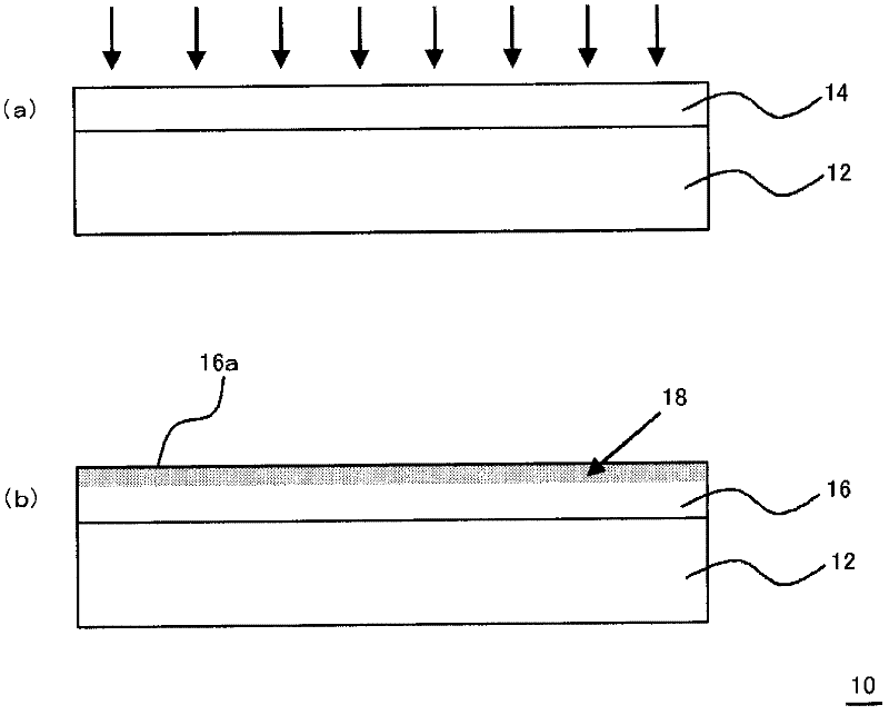
[0198] A 2 wt % xylene (dehydrated) solution of polysilazane (NL110A, manufactured by AZ Electronic Materials Co., Ltd.) was spin-coated (10 s, 3000 rpm) on a silicon substrate (thickness 530 μm, manufactured by Shin-Etsu Chemical Co., Ltd.). , and dried at 120° C. for 10 minutes to produce a polysilazane film with a thickness of 0.025 μm. Drying is carried out in an atmosphere with a water vapor concentration of about 500 ppm.
[0199] This polysilazane film was subjected to vacuum plasma treatment under the following conditions.
[0200] Vacuum plasma processing device: U-TEC Co., Ltd.
[0201] Gas: Ar
[0202] Gas flow: 50mL / min
[0203] Pressure: 19Pa
[0204] Temperature: room temperature
[0205] Applied power per electrode unit area: 1.3W / cm 2
[0206] Frequency: 13.56MHz
[0207] Treatment application: 5min
Embodiment 2
[0209] A 2 wt% xylene (dehydrated) solution of polysilazane (NN110A, manufactured by AZ Electronic Materials Co., Ltd.) without adding a catalyst was spin-coated (10s, 3000 rpm) on a silicon substrate (thickness 530 μm, manufactured by Shin-Etsu Chemical Co., Ltd.) , dried under the same conditions as in Example 1 to produce a polysilazane film with a thickness of 0.025 μm.
[0210] Then, vacuum plasma treatment was performed under the same conditions as in Example 1.
Embodiment 3
[0212] A 2 wt % xylene (dehydrated) solution of polysilazane (NL110A, manufactured by AZ Electronic Materials Co., Ltd.) was bar-coated on a polyethylene terephthalate (PET) film (thickness 50 μm, "A4100" Toyobo Co., Ltd.) was dried under the same conditions as in Example 1 to produce a polysilazane film with a thickness of 0.1 μm.
[0213] Then, vacuum plasma treatment was performed under the same conditions as in Example 1.
PUM
| Property | Measurement | Unit |
|---|---|---|
| thickness | aaaaa | aaaaa |
| thickness | aaaaa | aaaaa |
| thickness | aaaaa | aaaaa |
Abstract
Description
Claims
Application Information


