Method and apparatus for reducing leakage current in a read only memory device using pre-charged sub-arrays

a technology of read only memory and leakage current reduction, which is applied in the field of leakage current reduction of electronic memory devices comprised of arrays of transistors, can solve the problems of high leakage current, transistor sub-threshold leakage current, and significant leakage current of transistor sub-thresholds, so as to reduce leakage current and reduce leakage current

Active Publication Date: 2006-05-09
AVAGO TECH INT SALES PTE LTD
View PDF13 Cites 10 Cited by
  • Summary
  • Abstract
  • Description
  • Claims
  • Application Information

AI Technical Summary

Benefits of technology

[0006]Generally, a method and apparatus are provided for reducing leakage current in a read only memory device. The present invention reduces leakage current by precharging only a portion of the columns in a read only memory array during a given read cycle. In particular, the portion of the columns that are precharged is limited to a subset of columns that includes those columns that will be read during a given read cycle. The present invention recognizes that in a read cycle, where typically only a cell along the selected column will be read, only the corresponding column needs to be precharged.
[0007]In one implementation, a read column address is decoded to precharge only the portion of the columns of transistors that will be read during the given read cycle. In another variation, the columns of transistors are grouped into a plurality of sub-arrays and only those sub-arrays having columns that will be read during a given read cycle are precharged during the read cycle. Among other benefits, the reading operation of the present invention provides for faster operation and lower active current due to the smaller capacitances associated with smaller cell transistors. In addition, the power supply voltage drop is reduced due to high leakage current, thereby improving performance and reducing the need for wider power supply buses.

Problems solved by technology

As the size of ROM memory devices decrease, with improvements in integrated circuit fabrication technologies, the more narrow trace widths and shorter channel lengths of the ROM memory cell transistors can cause high leakage currents, referred to as transistor sub-threshold leakage current.
With more advanced CMOS technologies having trace widths of 0.16 μm or less, however, the transistor sub-threshold leakage current becomes a significant problem.
Such techniques, however, cause an undesirable increase in the physical size of the memory device, reduce the maximum frequency of operation and increase the active and standby currents.

Method used


Image

  • Method and apparatus for reducing leakage current in a read only memory device using pre-charged sub-arrays
  • Method and apparatus for reducing leakage current in a read only memory device using pre-charged sub-arrays
  • Method and apparatus for reducing leakage current in a read only memory device using pre-charged sub-arrays

Examples


Embodiment Construction

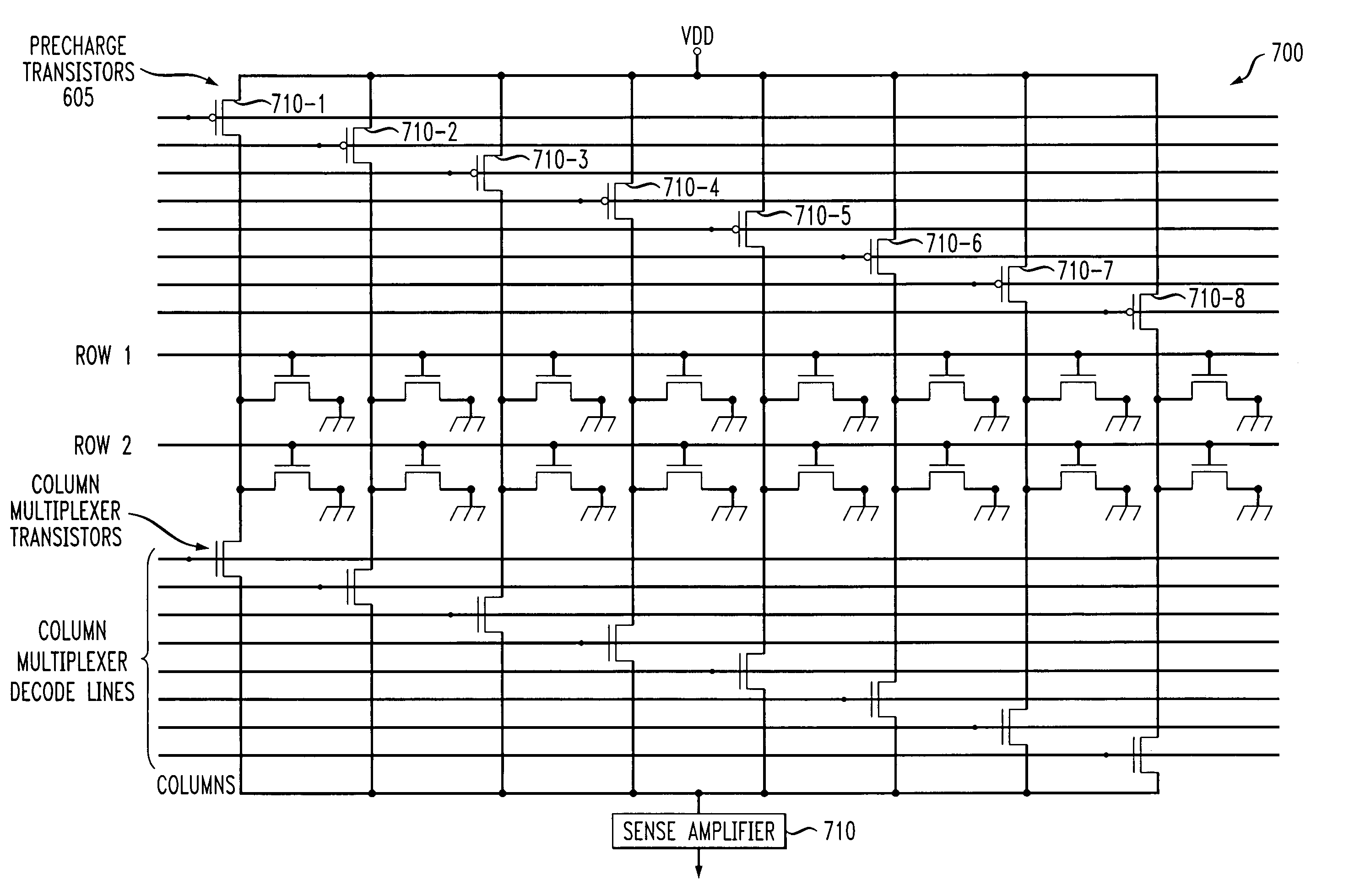
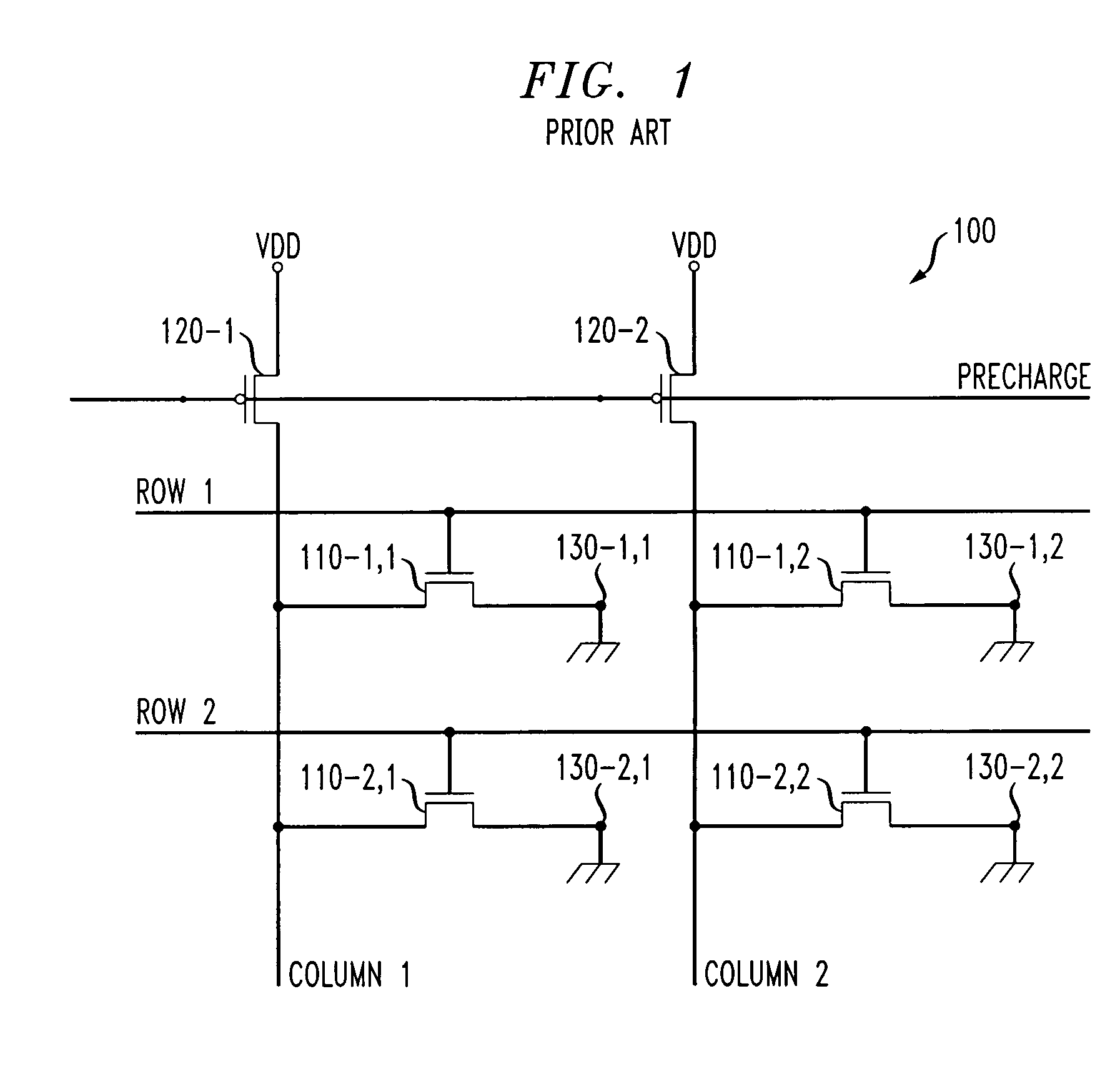
[0018]FIG. 1 illustrates a conventional ROM memory cell array with column precharge transistors. The memory cell transistors are n-channel transistors. The precharge transistors are p-channel devices. This type of ROM array is referred to as an “n-channel” array. There is also an analogous “p-channel” ROM memory array (not shown) where the cell transistors are p-channel transistors and the precharge transistors are n-channel transistors. For clarity, unless otherwise specified, all references and specified voltages herewithin apply to n-channel ROM memory arrays.

[0019]FIG. 1 illustrates a conventional n-channel two by two ROM array 100 of memory cells 110-l,l through 110-i,j. The memory cells 110-l,l through 110-i,j are generally comprised of n-channel transistors generally arranged in a grid pattern having a plurality (or series) of rows and columns. As shown in FIG. 1, the exemplary ROM array 100 includes a plurality, i, of rows (i=2), and a plurality, j, of columns (j=2). Each me...


PUM


Abstract

A method and apparatus are provided for reducing leakage current in a read only memory device. Leakage current is reduced by precharging only a portion of the columns in a read only memory array during a given read cycle. The portion of the columns that are precharged is limited to a subset of columns that includes those columns that will be read during a given read cycle. A read column address is decoded to precharge only the portion of the columns of transistors that will be read during the given read cycle. The columns of transistors can be grouped into a plurality of sub-arrays and only those sub-arrays having columns that will be read during a given read cycle are precharged during the read cycle.

Description

CROSS-REFERENCE TO RELATED APPLICATIONS[0001]The present application is related to U.S. patent application Ser. No. 10 / 764,150, entitled “Method and Apparatus for Reducing Leakage Current in a Read Only Memory Device Using Shortened Precharge Phase,” and U.S. patent application Ser. No. 10 / 764,000, entitled “Method and Apparatus for Reducing Leakage Current in a Read Only Memory Device Using Transistor Bias,” each filed contemporaneously herewith and incorporated by reference herein.FIELD OF THE INVENTION[0002]The present invention relates generally to electronic memory devices, and more particularly to the reduction of leakage current in electronic memory devices comprised of arrays of transistors.BACKGROUND OF THE INVENTION[0003]Data storage devices, such as read only memories (“ROMs”), typically store data in arrays of memory cells. Generally, a memory cell consists of a single transistor for each bit to be stored. The memory array is typically permanently programmed during the f...

Claims


Application Information

Patent Timeline
Patent Type & Authority Patents(United States)
IPC IPC(8): G11C7/00G11C7/12G11C17/12
CPCG11C17/12G11C7/12
Inventor DUDECK, DENNIS E.EVANS, DONALD ALBERTMCPARTLAND, RICHARD JOSEPHPHAM, HAI QUANG
Owner AVAGO TECH INT SALES PTE LTD
Why Eureka
Try Eureka