System, apparatus and method for contaminant reduction in semiconductor device fabrication equipment components

a technology of semiconductor devices and fabrication equipment, applied in valve housings, water supply installations, transportation and packaging, etc., can solve the problems of contamination, new components, and components that have been cleaned, and achieve the effects of improving the quality of semiconductor devices, and reducing the amount of contaminants

Active Publication Date: 2006-05-16
ATMEL CORP
View PDF17 Cites 11 Cited by
  • Summary
  • Abstract
  • Description
  • Claims
  • Application Information

AI Technical Summary

Benefits of technology

[0011]In one embodiment, the system and apparatus further include caps which are connectable to the manifold valves and to a type of component to undergo contaminant reduction having a pair of openings. When a component having two openings, such as a ball valve or a pressure control valve, is connected to a manifold valve for contaminant reduction, one end of the component is connected to the manifold valve at an end having a first opening and the other end of the component having a second opening is capped with a cap to maintain the vacuum within the manifold by preventing atmospheric particles from entering the component and manifold. When the component is a rotation assembly, one end of the rotation assembly including an opening is connected to the manifold valve, while the other end is typically already closed and thus does not require a cap. When a component is not connected to a particular manifold valve, an uncovered manifold valve opening may be capped to maintain the vacuum within the system when the valve is in an open position.
[0015]The apparatus and system of the present invention is advantageous in at least that it reduces the amount of contaminants, such as oxygen, found on surfaces of semiconductor device fabrication equipment components. A reduction in oxygen within the components will result in an improvement in the quality of semiconductor devices manufactured by the equipment.
[0016]Furthermore, the present invention may reduce contaminants of more than one component and more than one type of component at a time. These components may be connected to the manifold valves, found within the oven, or both.
[0017]Additionally, reduction of contaminants on components, with the system, apparatus, and method of the present invention, makes future removal of contaminants easier to achieve. Therefore, preventative maintenance recovery time, process recovery time, and mean time to repair (MTTR) are reduced. Further, mean time between interrupt (MTBI) of operation and mean time between cleans (MTBC) will increase as the semiconductor fabrication device equipment will not need to be maintained as often if contaminant reduction has been achieved with the present invention.

Problems solved by technology

Semiconductor device fabrication equipment components tend to accumulate contaminants, through for example, adsorption and absorption, before, during, and / or after the operation of the fabrication equipment.
Even components that have been cleaned, by cleaning processes known in the art, or that are new, are subject to accumulation of contaminants.
Thus, the components of the semiconductor device fabrication equipment become a source of contaminants, in addition to process gases.
Contaminants on components are undesirable for at least the reasons that they degrade the quality of the fabricated semiconductor device manufactured and reduce the efficiency of the fabrication process.
Elevated oxygen levels present in the CVD reaction chamber used to deposit SiGe causes numerous problems in the SiGe films produced in the CVD reactor chamber.
Among these problems are elevated sheet resistance of the SiGe p-type base and poor crystal quality.
The longer the reactor is offline, the less cost effective manufacturing becomes, as an offline reactor cannot be used for manufacturing semiconductor chips.
Also, elevated contaminant levels in the reactor components may lead to early reactor failure and a decreased reactor lifetime.

Method used


Image

  • System, apparatus and method for contaminant reduction in semiconductor device fabrication equipment components
  • System, apparatus and method for contaminant reduction in semiconductor device fabrication equipment components
  • System, apparatus and method for contaminant reduction in semiconductor device fabrication equipment components

Examples


Embodiment Construction

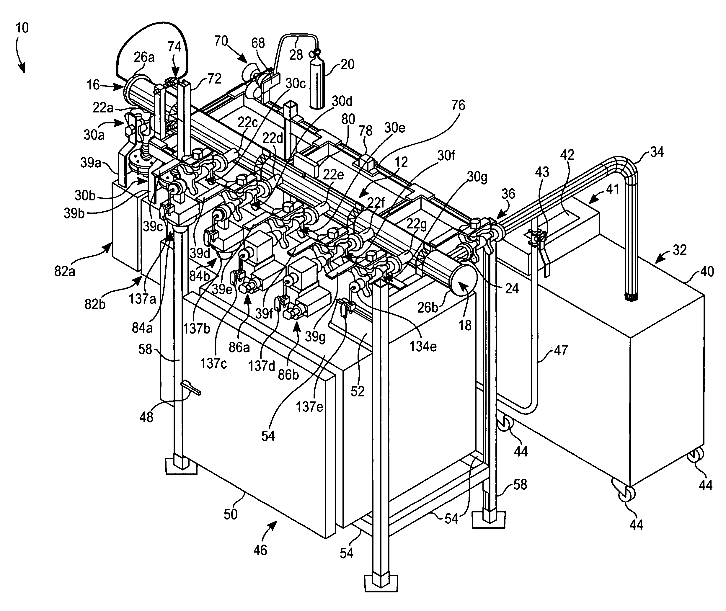
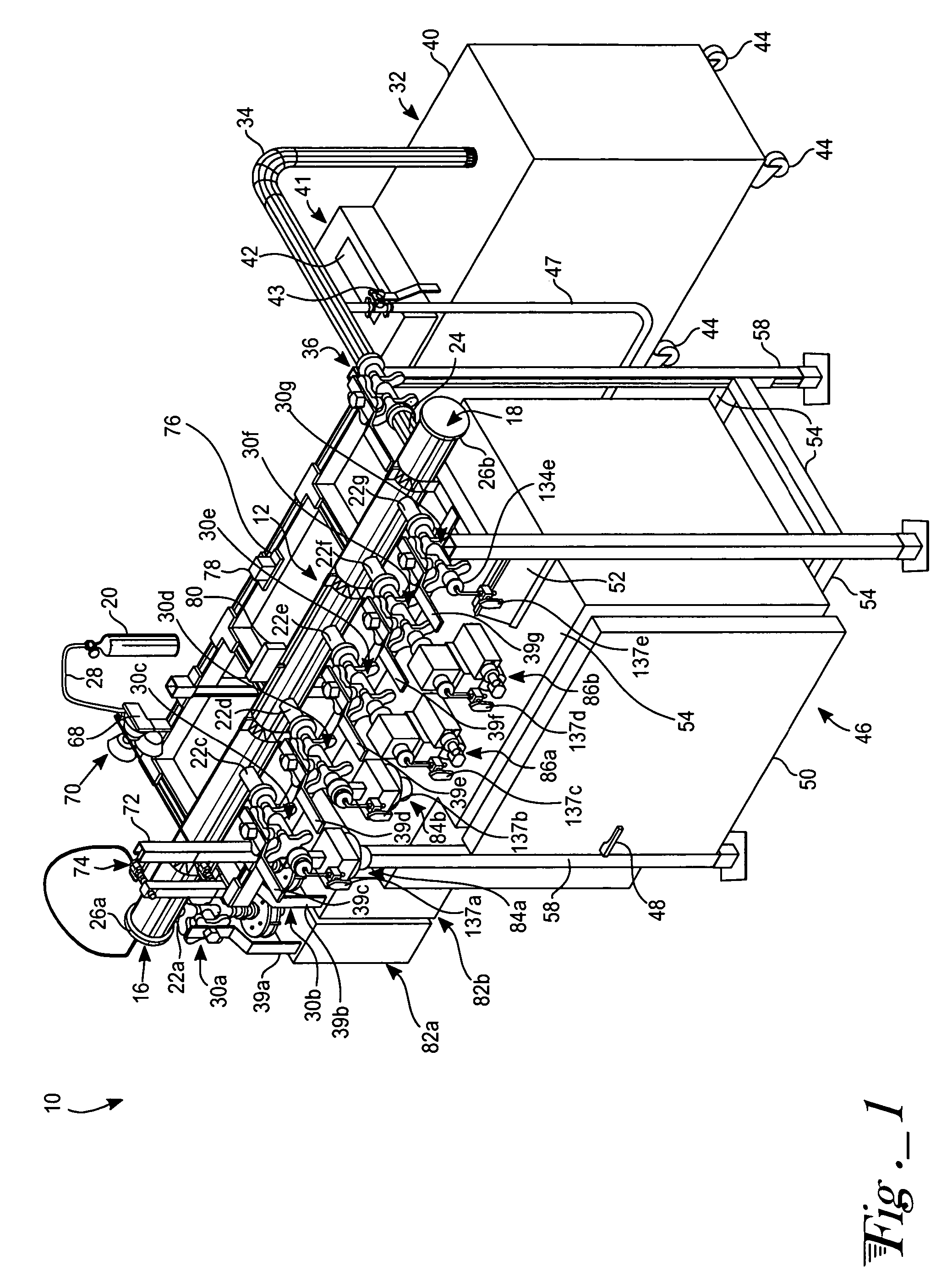
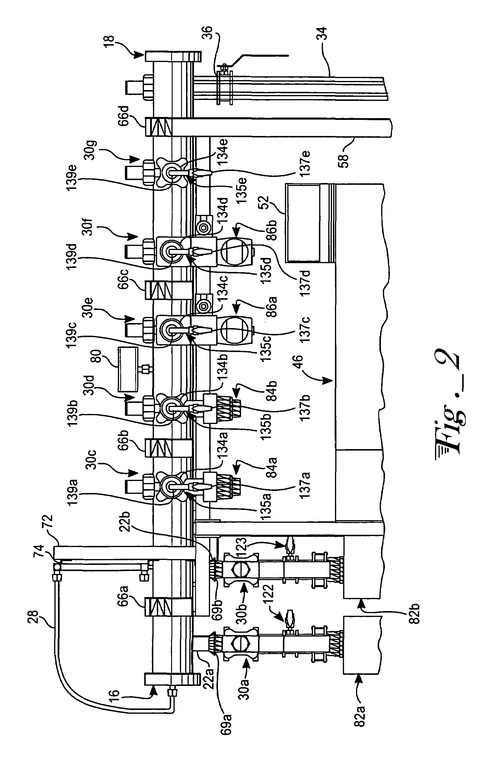
[0030]With reference to FIG. 1, the system 10 of the present invention is seen featuring a manifold 12. Referring to FIG. 1 and FIGS. 5a–c, the manifold 12 is, for example, a stainless steel pipe, having a length of, for example, 178 cm (70⅛ inches). The manifold 12 includes a main internal passageway 14 capped with first and second capped ends 16 and 18 (cap 18 is not shown in FIG. 5a), the first capped end 16 appearing as capped end 18 except for having an opening (not shown) connected to a fluid source 20, a plurality of inlets 22a–22g disposed in between the capped ends 16 and 18 and in fluid communication with the main passageway 14, and an exhaust fitting 24 disposed proximate to the second capped end 18 and downstream from the plurality of inlets 22a–22g, the exhaust fitting 24 being in fluid communication with the main passageway 14 and the inlets 22a–22g. Capped end 16 includes flange 26a and capped end 18 includes flange 26b. For example, flanges 26a and 26b are NW100 flan...


PUM


Abstract

A system, apparatus, and method for reducing contaminants of semiconductor device fabrication equipment components, featuring a manifold having a passageway in fluid communication with to a plurality of inlets and for providing a purge fluid to removably connected components to undergo contaminant reduction. The inlets are connected to a plurality of manifold valves to which components are removably connected. The manifold valves are operable to place connected components into and out of fluid communication with the inlets and the passageway. A fluid source supplies purge fluid to the manifold and a pump is connected to the manifold to remove fluid from the system. In one embodiment an oven is connected to the system for outgassing and for reduction of moisture in additional components.

Description

FIELD OF THE INVENTION[0001]The invention relates to semiconductor device fabrication equipment in general, and, in particular, to a system, apparatus, and method for contaminant reduction of semiconductor device fabrication equipment components.BACKGROUND OF THE INVENTION[0002]Semiconductor device fabrication equipment components tend to accumulate contaminants, through for example, adsorption and absorption, before, during, and / or after the operation of the fabrication equipment. Such contaminants include, for example, moisture, oxygen, atmosphere, or any other gases. Possible contaminant sources are process gases as well as the atmosphere. Even components that have been cleaned, by cleaning processes known in the art, or that are new, are subject to accumulation of contaminants. Thus, the components of the semiconductor device fabrication equipment become a source of contaminants, in addition to process gases. Contaminants on components are undesirable for at least the reasons th...

Claims


Application Information

Patent Timeline
Patent Type & Authority Patents(United States)
IPC IPC(8): F16K11/00F16K27/00
CPCF16K27/003Y10T137/0318Y10T137/4259Y10T137/85978Y10T137/87877
Inventor ENICKS, DARWIN G.FRIEDRICHS, CARL E.BRUCHER, RICHARD A.
Owner ATMEL CORP
Why Eureka
Try Eureka