Bonding apparatus with position deviation correction

Active Publication Date: 2006-05-16
SHINKAWA CO LTD
View PDF9 Cites 14 Cited by
  • Summary
  • Abstract
  • Description
  • Claims
  • Application Information

AI Technical Summary

Benefits of technology

[0024]One object of the present invention is to solve such problems encountered in the prior

Problems solved by technology

Accordingly, if there is a shift in these optical axes, this has an effect on positioning, and causes positional deviation in the bonding.
H6-28272 requires two targets; furthermore, the work of adjusting and aligning the positional relationship between these targets is required, so that the construction is complicated, and the work takes time.
Even assuming that the amount of deviation +Xc between the optical axis of the first camera and the optical axis of the second camera can be accurately measured and corrected, when the bonding work is performed, positional deviation in the bonding occurs in cases where the bonding tool does not move parallel to the optical axis to the bonding height on the substrate from the positioning height of the bonding tool, so that the chip cannot be accurately disposed on the substrate.
However, what can be measured by trial bonding is the amount of deviati

Method used


Image

  • Bonding apparatus with position deviation correction
  • Bonding apparatus with position deviation correction
  • Bonding apparatus with position deviation correction

Examples


embodiment 1

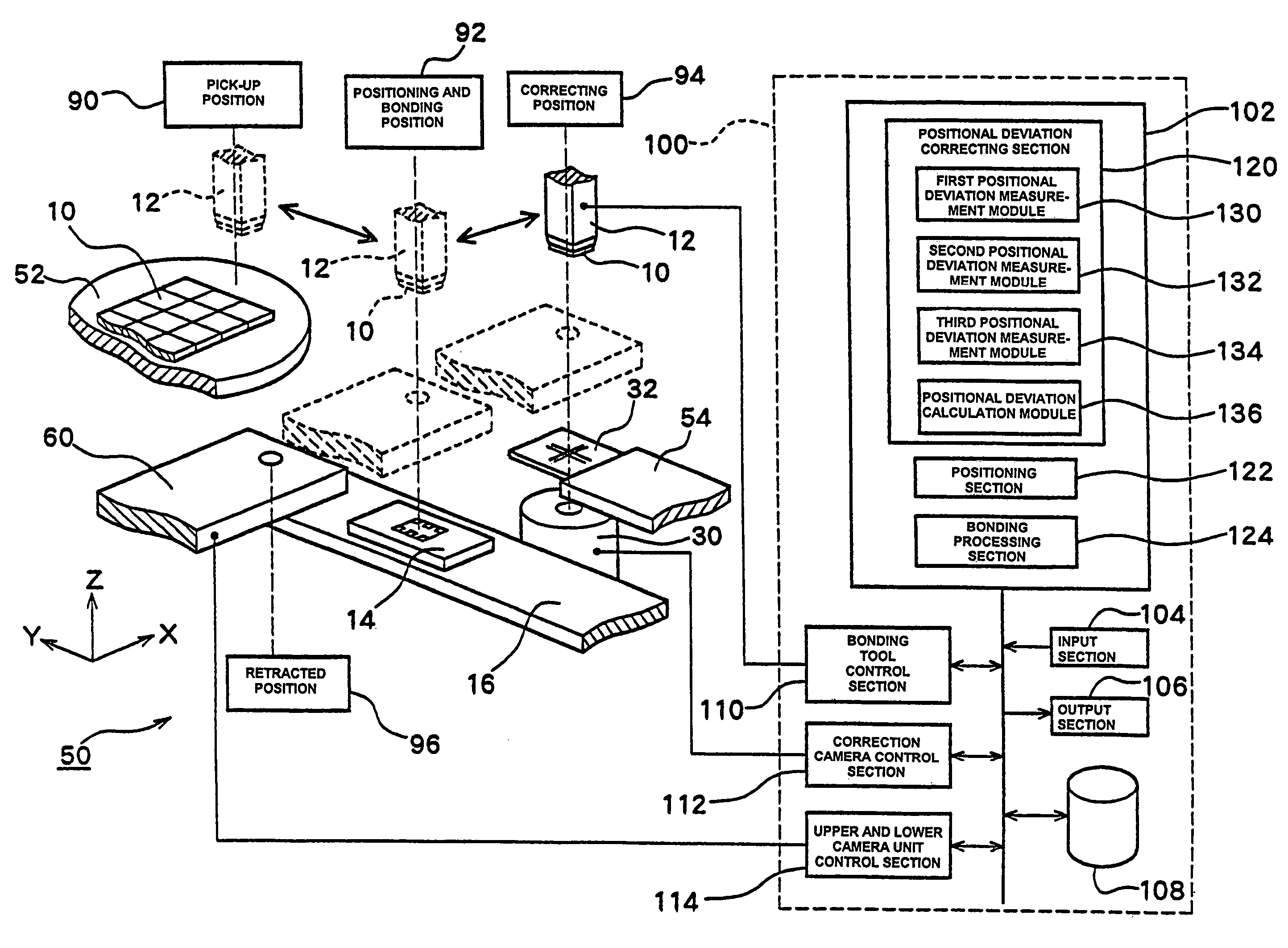
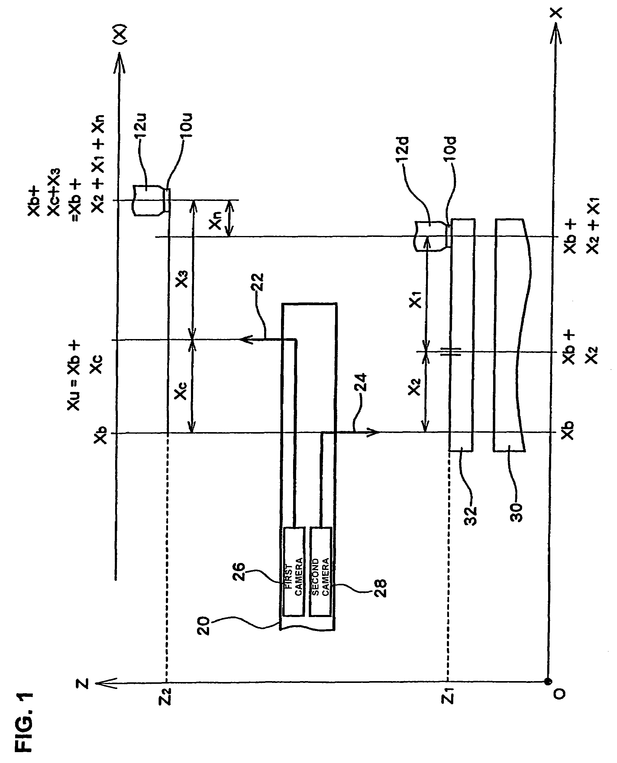
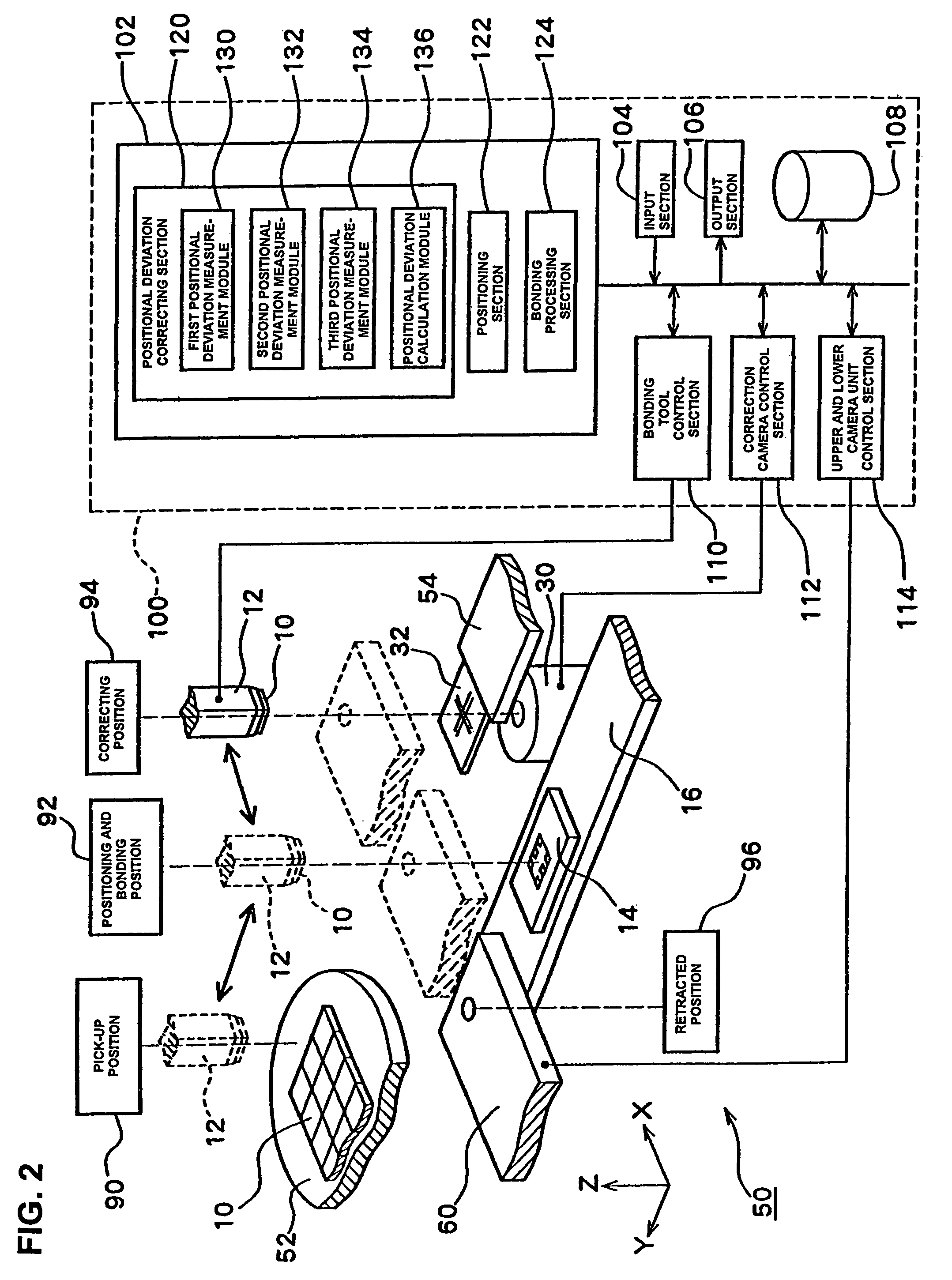
[0169]FIG. 2 is a structural diagram of the bonding apparatus 50.

[0170]The bonding apparatus 50 comprises a bonding tool 12 which holds the back side of a chip 10 by vacuum suction, etc., a carrier 16 which holds and conveys the substrate 14, a supply station 52 which supplies chips 10, upper and lower camera unit 60 which detects the positions of the substrate 14 and chip 10, a correction camera 30 which is used to correct the positional deviation in bonding, a target 32 (used as a position reference) which is held in a target holder 54, and a control device 100 which controls the operations of these elements.

[0171]The bonding tool 12 is a member with the shape of a square pyramid which has a chip holding part on the tip end. A vacuum suction hole which communicates with the chip holding part is formed in the center, and suction holding of the chip 10 can be accomplished in the chip holding part under the control of the control device 100. Furthermore, the bonding tool 12 is connec...

embodiment 2

[0203]Instead of the bonding apparatus with the above-described construction shown in FIG. 2, a bonding apparatus in which a combination of the second camera with a separate optical part is endowed with the function of the correction camera may be constructed.

[0204]FIG. 14 is a diagram which shows in model form a top view layout of the main constituent elements of a bonding apparatus 200 in which an optical part 202 that conducts an image of the target 32 to the second camera 28 is used instead of the correction camera. FIG. 15 is a diagram which shows in model form a side view layout of these constituent elements. The same symbols are assigned to elements that are the same as in FIG. 2, and a detailed description of such elements is omitted. The bonding apparatus 200 comprises a target 32, and an optical part 202 that is disposed beneath the substrate 14 and carrier 16. The optical part 202 includes a prism 204 which is disposed beneath the target 32, a prism 206 which is disposed ...

embodiment 3

[0207]Furthermore, instead of the bonding apparatus with the above-described construction shown in FIG. 2, a bonding apparatus in which the imaging reference position of the correction camera is endowed with the function of the position reference of the target may be constructed. FIG. 17 is a diagram which shows in model form a top view layout of the main constituent elements of a bonding apparatus 220 in which the imaging reference position of the correction camera 30 is used as the position reference. FIG. 18 is a diagram which shows in model form a side view layout of these constituent elements. Embodiment 3 differs from that shown in FIG. 2 in that no target 32 is installed.

[0208]By using the imaging reference position of the correction camera 30 as the position reference, it is possible to determine the correction amount Δ(X, Y) for correcting the positional deviation in bonding without using a target.

[0209]FIG. 19 is a diagram which shows the conditions of determination of the...


PUM

PropertyMeasurementUnit
Angleaaaaaaaaaa
Heightaaaaaaaaaa
Distanceaaaaaaaaaa

Abstract

A bonding apparatus that makes correction ΔX=(Xn−Xc) in positioning of bonding tool and substrate where the imaging center of first camera shows deviation +Xc with respect to the imaging center of second camera, and deviation +Xn occurs when bonding tool moves from height Z1 to height Z2. A target is disposed at height Z1 in a correcting position, and a correction camera is disposed beneath the target. The correction amount ΔX=(Xn−Xc)=X3−(X2+X1) is determined based upon first positional deviation X1 which is the position of a chip 10d at height Z1 seen from the target, second positional deviation X2 which is the position of the target seen from the imaging center of the second camera, and third positional deviation X3 which is the position of the chip 10u at height Z2 seen from the imaging center of the first camera.

Description

BACKGROUND OF THE INVENTION[0001]1. Field of the Invention[0002]The present invention relates to a bonding apparatus and more particularly to a bonding apparatus which has a positioning mechanism for aligning the position of a bonding tool and the position of a substrate.[0003]2. Prior Art[0004]In addition to wire bonding, face-down bonding is performed as a mounting method for connecting the bonding pads on chips such as LSI device, etc., and the bonding leads of substrates. Face-down bonding is a method in which the back surface side of the chip is held by the bonding tool, the front surface side of the held chip (i.e., the surface on the side on which electrode pads are disposed) and the wiring surface of the substrate are caused to face each other, the positions of the electrode pads on the chip and the positions of the bonding leads of the substrate are aligned, and these pads and leads are connected using thermal energy or ultrasonic energy. Flip-chip bonders and COF (chip on ...

Claims


Application Information

Patent Timeline
IPC IPC(8): B32B41/00G06T1/00G05G15/00H01L21/60
CPCH01L24/75H01L24/81H01L2224/75H01L2224/75745H01L2224/75753H01L2224/81121H01L2924/12041H01L2224/81801H01L2924/01051H01L2924/01082H01L2924/01006H01L2924/01033H01L2224/81205H01L21/60
Inventor HARAGUCHI, MANABU
Owner SHINKAWA CO LTD
Why Eureka
Try Eureka