Optical proximity correction method and manufacturing method of mask

A technology for optical proximity correction and reticle, which is applied in optics, originals for opto-mechanical processing, and photo-engraving processes on pattern surfaces, which can solve the problems of low accuracy of optical proximity correction and achieve high precision.

Active Publication Date: 2019-08-13
SEMICON MFG INT (SHANGHAI) CORP +1
View PDF6 Cites 10 Cited by
  • Summary
  • Abstract
  • Description
  • Claims
  • Application Information

AI Technical Summary

Problems solved by technology

[0005] However, the correction accuracy of o...

Method used


Image

  • Optical proximity correction method and manufacturing method of mask
  • Optical proximity correction method and manufacturing method of mask
  • Optical proximity correction method and manufacturing method of mask

Examples


Embodiment Construction

[0028] As mentioned in the background, the existing optical proximity correction method has poor accuracy.

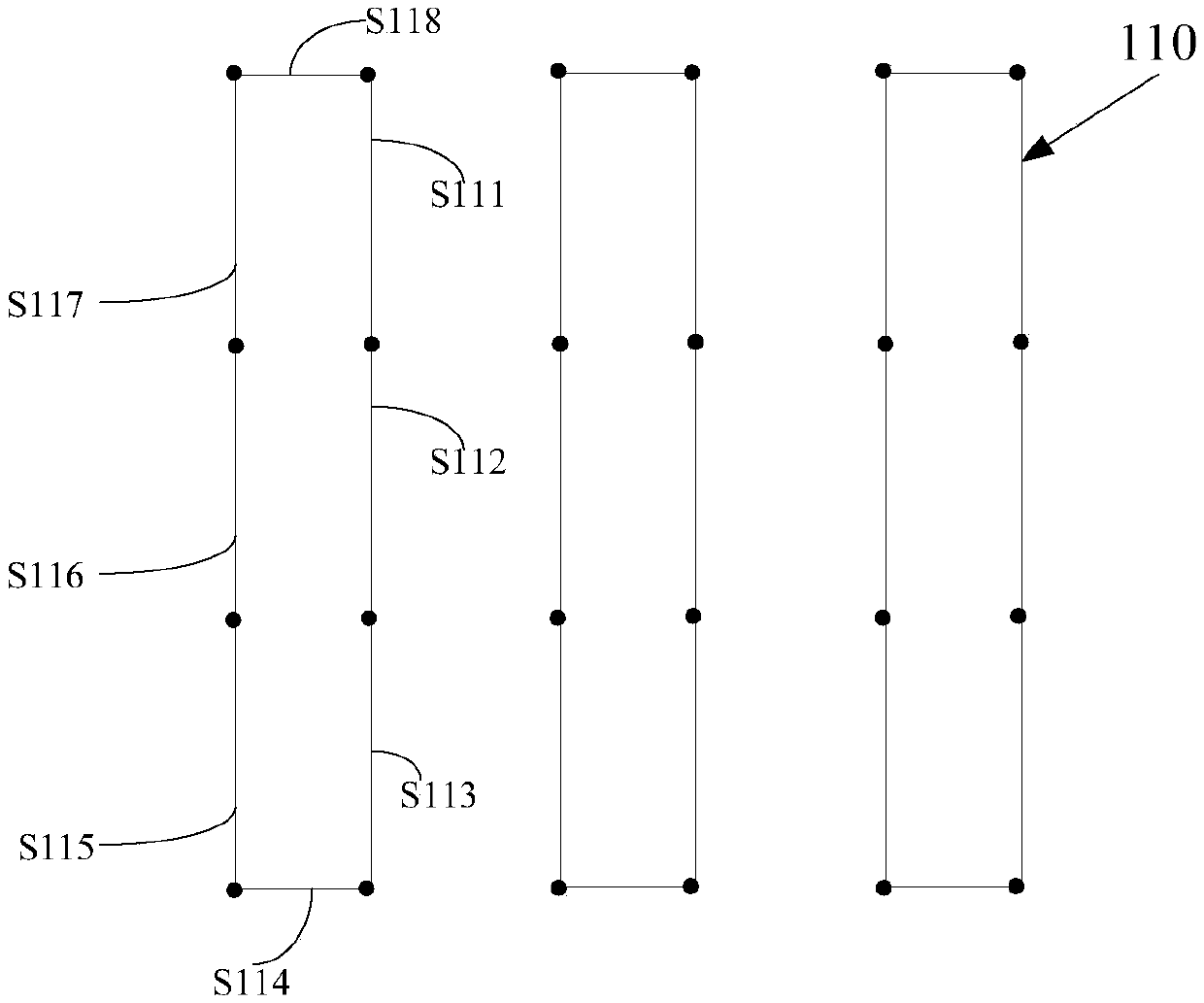
[0029]An optical proximity correction method, comprising: providing a target etching pattern, the target etching pattern including a plurality of sub-target etching patterns; obtaining a mask layer pattern corresponding to the sub-target etching pattern according to an etching offset table; The OPC correction is performed on the film layer graphics to obtain the corrected graphics.

[0030] A mask is made with the corrected pattern, and actual exposure is performed on the mask to obtain an actual exposure pattern, and there is a certain positional deviation between the actual exposure pattern and the previous layer pattern. The above positional deviation is usually caused by the thermal expansion of the target etching pattern during the process and the positional deviation of the mask. However, the process of performing OPC correction on the pattern of the mask layer d...


PUM


Abstract

The invention discloses an optical proximity correction method and a manufacturing method of a mask, and the method comprises the steps: providing a target etching pattern which comprises a pluralityof sub-target etching patterns; providing an offset compensation model; dividing each edge of the sub-target etching pattern into a plurality of segmentation edges; according to the offset compensation model, performing compensation correction on each segmentation edge to obtain a compensation graph; obtaining a mask layer graph corresponding to the compensation graph; and performing OPC correction on the mask layer pattern to obtain a corrected pattern. According to the optical proximity correction method, the correction precision is improved.

Description

technical field [0001] The invention relates to the field of semiconductor manufacturing, in particular to an optical proximity correction method and a mask plate manufacturing method. Background technique [0002] Photolithography technology is a crucial technology in semiconductor manufacturing technology. Photolithography technology can realize the transfer of graphics from the mask to the surface of the silicon wafer to form semiconductor products that meet the design requirements. The photolithography process includes an exposure step, a development step performed after the exposure step, and an etching step after the development step. In the exposure step, light is irradiated onto the silicon wafer coated with photoresist through the light-transmitting area of ​​the mask, and the photoresist reacts chemically under the irradiation of light; The photoresist is different to the degree of dissolution of the developer, forming a photoresist pattern, and realizing the tran...

Claims


Application Information

Patent Timeline
IPC IPC(8): G03F1/36
CPCG03F1/36
Inventor 杜杳隽
Owner SEMICON MFG INT (SHANGHAI) CORP
Why Eureka
Try Eureka