Page buffer of flash memory device and data program method using the same

a flash memory device and data program technology, applied in static storage, digital storage, instruments, etc., can solve the problems of low affecting the operation speed of the device, and consuming a lot of time, so as to achieve the effect of improving the operating speed of the devi

Active Publication Date: 2006-05-16
STMICROELECTRONICS SRL +1
View PDF3 Cites 33 Cited by
  • Summary
  • Abstract
  • Description
  • Claims
  • Application Information

AI Technical Summary

Benefits of technology

[0018]Accordingly, the present invention has been made in view of the above problems, and it is an object of the present invention to provide a page buffer of a flash memory device and a data program method using the same in which the number and time of operations for data loading, program and program verification can be reduced by half and the operating speed of the device can be improved, in such a manner that after two data are sequentially stored in a main register (first latch) and a cache register (second latch) provided in a page buffer, they are transferred to an even bit line and an odd bit line, respectively, at the same time, and a bias needed for a program is applied to cells connected to the even bit line and the odd bit line, respectively, to perform the program at the same time.

Problems solved by technology

Thus, during the program operation, lots of time is consumed.
Therefore, there are problems in that lots of a program time is consumed and the operating speed of a device becomes thus low.

Method used


Image

  • Page buffer of flash memory device and data program method using the same
  • Page buffer of flash memory device and data program method using the same
  • Page buffer of flash memory device and data program method using the same

Examples


Embodiment Construction

[0027]Now the preferred embodiments according to the present invention will be described with reference to the accompanying drawings. Since preferred embodiments are provided for the purpose that the ordinary skilled in the art are able to understand the present invention, they may be modified in various manners and the scope of the present invention is not limited by the preferred embodiments described later.

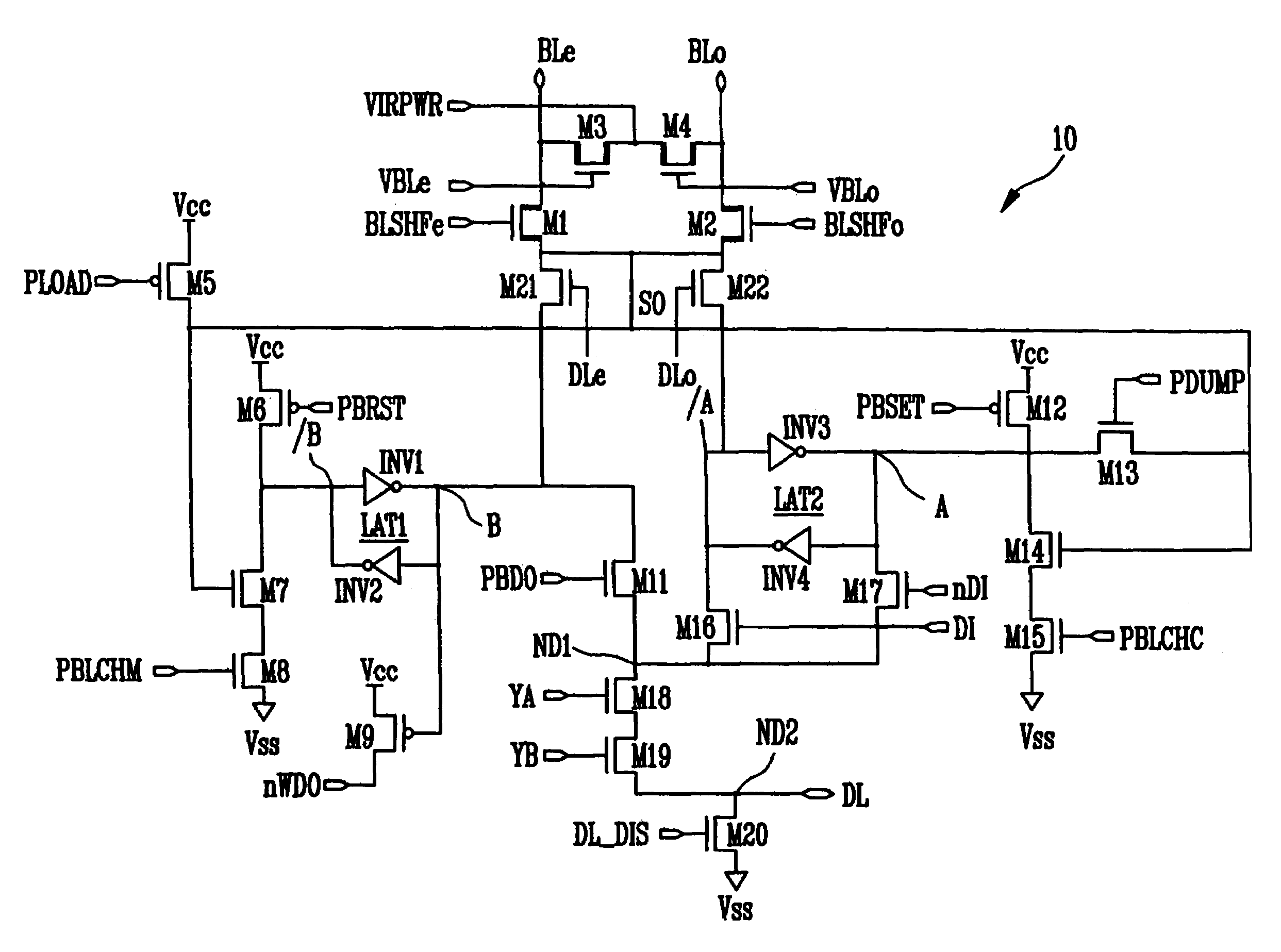
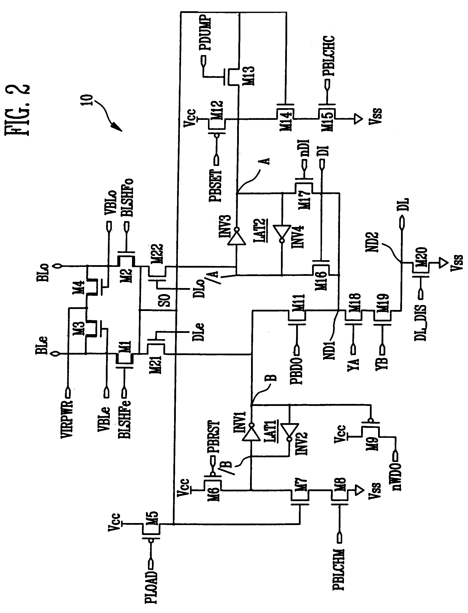
[0028]FIG. 2 is a circuit diagram showing a page buffer of a flash memory device according to an embodiment of the present invention.

[0029]Referring to FIG. 2, the page buffer 10 of the flash memory device according to an embodiment of the present invention is connected to a pair of bit lines BLe and BLo. A NMOS transistor M1 is connected between the bit line BLe and a sense node SO. The NMOS transistor M1 is controlled by a control signal BLSHFe. A NMOS transistor M2 is connected between the bit line BLo and the sense node SO. The NMOS transistor M2 is controlled by a control ...


PUM


Abstract

Disclosed are a page buffer of a flash memory device and data program method using the same. After two data are sequentially stored in a main register (first latch) and a cache register (second latch) provided in a page buffer, they are respectively transferred to an even bit line and an odd bit line at the same time, and a bias needed for a program is applied to cells connected to the even bit line and the odd bit line, respectively, whereby the program is performed at the same time. Therefore, the number and time of operations for data loading, program operation and program verification can be reduced by half and the operating speed of the device can be improved.

Description

[0001]This application relies for priority upon Korean Patent Application No. 2004-0038468 filed May 28, 2004, the contents of which are herein incorporated by reference in their entirety.BACKGROUND[0002]1. Field of the Invention[0003]The present patent relates to a page buffer of a flash memory device and a data program method using the same, and more specifically, to a page buffer of a flash memory device in which a program speed can be improved and a data program method using the same.[0004]2. Discussion of Related Art[0005]In a NAND flash memory device, in order to program data, one data is loaded onto a page buffer and the loaded data is transferred to a bit line wherein an erased cell will be programmed. Thus, in the case where several pages are to be programmed, one data is loaded onto the page buffer, a cell is programmed according to the loaded data and the data is then stored. Next, in order to store data in a next page, data is loaded onto the page buffer and a cell is pr...

Claims


Application Information

Patent Timeline
Patent Type & Authority Patents(United States)
IPC IPC(8): G11C16/04G11C16/02G11C16/06G11C16/10
CPCG11C16/10G11C2216/14G11C5/063G11C16/24
Inventor LEE, JU YEAB
Owner STMICROELECTRONICS SRL
Why Eureka
Try Eureka