Bus connection circuit for read operation of multi-port memory device

a multi-port memory and bus connection technology, applied in the direction of hollow article cleaning, refuse collection, instruments, etc., can solve the problems of power consumption and the inability of the pull-up driver to meet the area of the semiconductor memory chip,

Active Publication Date: 2006-05-16
SK HYNIX INC
View PDF5 Cites 13 Cited by
  • Summary
  • Abstract
  • Description
  • Claims
  • Application Information

AI Technical Summary

Problems solved by technology

However, in recent years, a function separation between the memory device and the chipset has been ambiguous and an integration of the chipset and the memory device has been considered.
However, in case where the number of the global data bus lines is more than 64, for example, 128, 256 or 512, a large amount of current is consumed during data transmission, thus causing a problem of power consumption.
For this reason, the pull-up driver is not suitable in view of an area of the semiconductor memory chip.

Method used


Image

  • Bus connection circuit for read operation of multi-port memory device
  • Bus connection circuit for read operation of multi-port memory device
  • Bus connection circuit for read operation of multi-port memory device

Examples


Embodiment Construction

[0083]Hereinafter, the present invention will be described in detail with reference to the accompanying drawings.

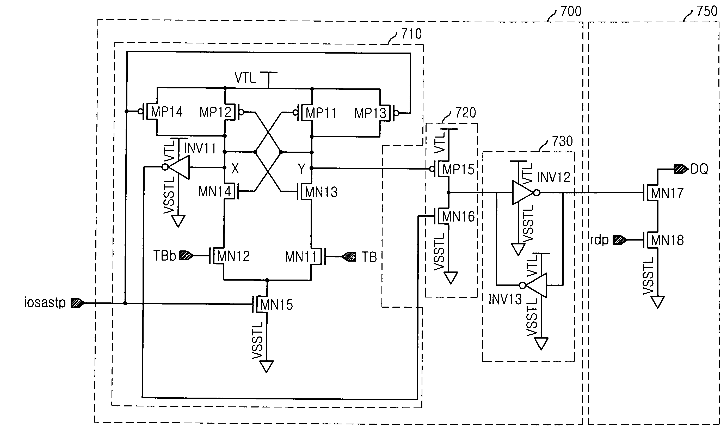
[0084]FIG. 7 is a circuit diagram of a bus connection circuit for a read operation of a multi-port DRAM in accordance with an embodiment of the present invention.

[0085]Referring to FIG. 7, a bus connection circuit for a read operation of a multi-port DRAM in accordance with an embodiment of the present invention includes a read data sensing / latching block 700 and a read data driving block 750. The read data sensing / latching block 700 senses / latches read data of transfer buses TB and TBb in response to a read data strobe signal iosastp. The read data driving block 750 drives data latched by the read data sensing / latching block 700 to a global data bus in response to a read data driving pulse rdp. Also, the read data driving block 750 connects or disconnects a path of current flowing the global data bus according to a logic level of the latched data.

[0086]Here, the read dat...


PUM


Abstract

There is provided a semiconductor memory design technique, specifically a bus connection circuit for a read operation of a multi-port memory device. The bus connection circuit is adapted to a current sensing type bus transmission / reception structure. The bus connection circuit includes: a read data sensing / latching unit for sensing / latching a read data applied on a local data bus in response to a read data strobe signal; and a read data driving unit for driving the data latched in the read data sensing / latching unit to a global data bus in response to a read data driving pulse, and for connecting or disconnecting a path of current flowing the global data bus according to a logic level of the latched data.

Description

FIELD OF THE INVENTION[0001]The present invention relates to a semiconductor memory design technology; and, more particularly, to a bus connection circuit for a read operation of a multi-port memory device.DESCRIPTION OF RELATED ART[0002]Most of memory devices, including a random access memory (RAM), have one port. Also, one port has a plurality of input / output pin sets. In other words, the memory device has only one port for data exchange with chipset. However, in recent years, a function separation between the memory device and the chipset has been ambiguous and an integration of the chipset and the memory device has been considered. This tendency demands a multi-port memory device that can directly exchange data with peripheral graphic devices, CPU, and so on. In order to implement such a multi-port memory device, any one of a plurality of ports must be able to provide an access to all memory cells.[0003]FIG. 1 is a block diagram illustrating an architecture of a 256M multi-port ...

Claims


Application Information

Patent Timeline
Patent Type & Authority Patents(United States)
IPC IPC(8): G11C8/00G11C5/06G11C7/06G11C7/10G11C8/16G11C11/4091G11C11/4096
CPCG11C7/1069G11C7/1075G11C8/16G11C11/4091G11C7/1051G11C5/063G11C7/065G11C7/1048G11C11/4096G11C2207/002E04F17/123B08B5/02B08B9/027B65F5/005
Inventor SHIN, BEOM-JU
Owner SK HYNIX INC
Why Eureka
Try Eureka