Paste including a mixture of powders, connection plug, burying method, and semiconductor device manufacturing method

a technology of burying method and paste, which is applied in the direction of semiconductor devices, semiconductor/solid-state device details, electrical apparatus, etc., can solve the problem that the trench cannot be filled with paste, and achieve the effect of easy removal, and increasing the width of the trench

Inactive Publication Date: 2006-05-23
KK TOSHIBA
View PDF16 Cites 3 Cited by
  • Summary
  • Abstract
  • Description
  • Claims
  • Application Information

AI Technical Summary

Benefits of technology

[0029]In the present invention, the excess portion of the paste is removed in the step of temporarily hardening the paste, in which the paste can be easily removed, instead of the step after calcination in which the paste is difficult to remove. Even if, therefore, the width of the trench increases, and the amount of paste increases, an excess paste portion can be removed without taking much time.
[0030]According to the present invention, therefore, even if the width of the trench is increased to decrease the resistance of the connection plug, an increase in the formation time of a connection plug made of a paste can be suppressed.

Problems solved by technology

If the volume reduction of the paste is large, the trench cannot be filled with the paste.

Method used


Image

  • Paste including a mixture of powders, connection plug, burying method, and semiconductor device manufacturing method
  • Paste including a mixture of powders, connection plug, burying method, and semiconductor device manufacturing method
  • Paste including a mixture of powders, connection plug, burying method, and semiconductor device manufacturing method

Examples


first embodiment

(First Embodiment)

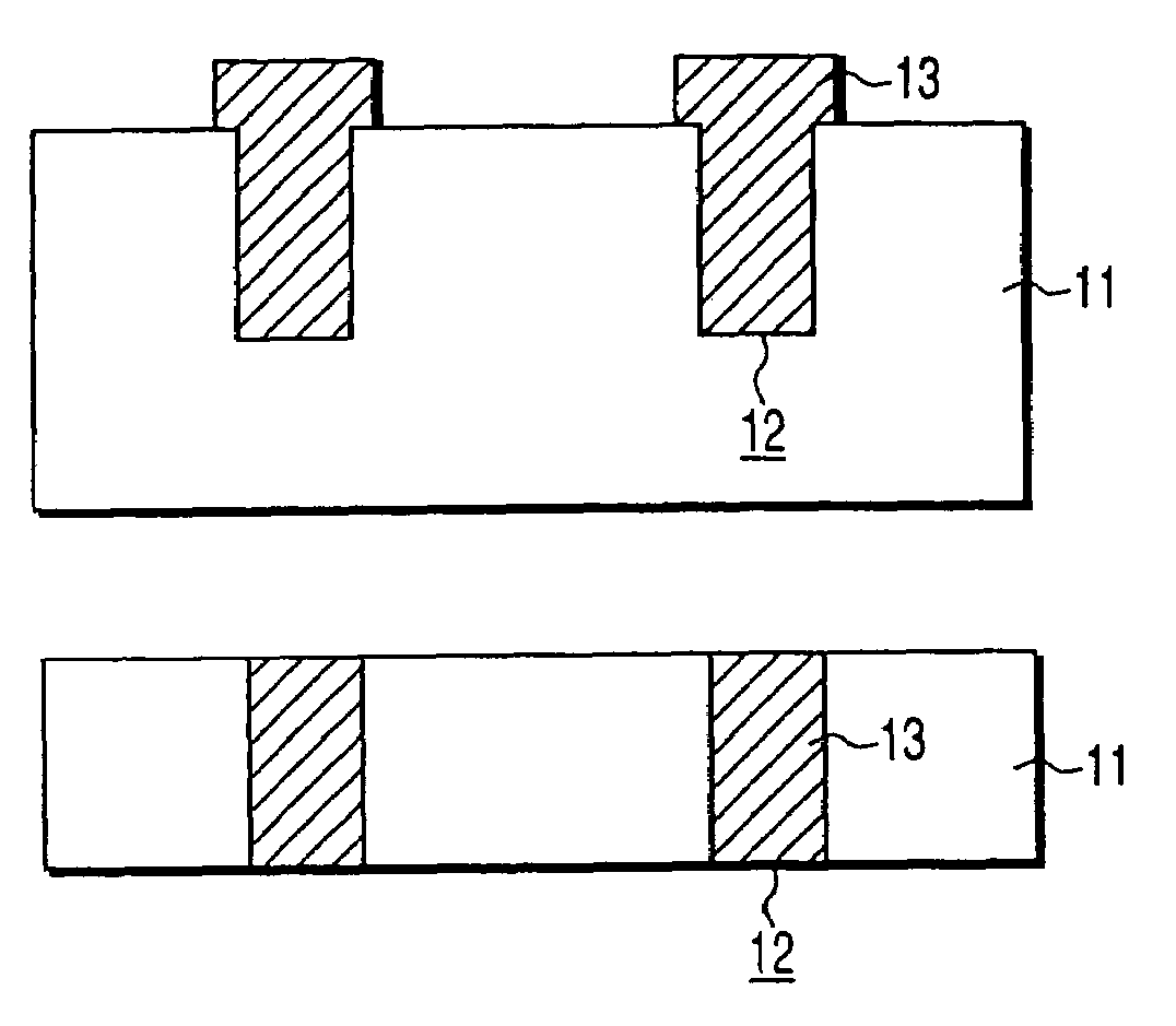
[0058]In this embodiment, a paste is buried in a trench formed in the surface of a substrate by a printing method using a squeegee. In the conventional method, as shown in FIGS. 5A and 5B, voids and recesses were formed in trenches because a paste is not sufficiently buried in the trenches.

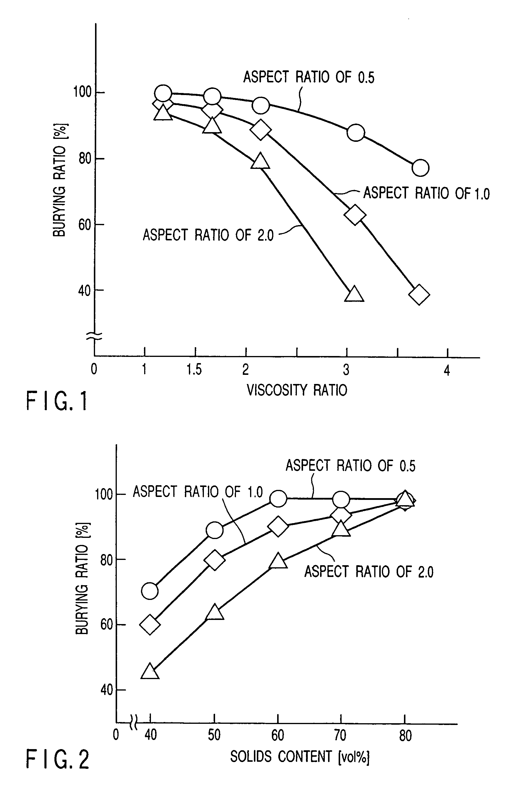
[0059]The present inventors found that the causes of this problem were a change in the viscosity of the paste when buried with the squeegee and the shrinkage of the paste upon volatilization (to be referred to as hardening hereinafter) of the solvent of the paste. To improve the buried shape of a paste, this embodiment therefore uses a paste for which a viscosity change upon burial and a solids content are controlled.

[0060]FIG. 1 shows the relationship between the viscosity ratio of a paste and the burying ratio of a viahole. In this case, the viahole has a depth of 50 to 200 μm and an opening diameter of 100 μm. The paste was buried under the condition that the viscosity measure...

second embodiment

(Second Embodiment)

[0085]In this embodiment, a chip-through plug (connection plug) for a multichip module is formed by using a paste having excellent burying characteristics as in the first embodiment.

[0086]The following conditions are required for a chip-through plug. The chip-through plug must be sufficiently buried in a trench to allow the chip to make lower-surface contact. The upper portion of the chip-through plug (to be referred to as the plug upper portion hereinafter) must be flat to allow an interconnection to be formed on the plug upper portion. The lower portion of the chip-through plug (to be referred to as the plug lower portion hereafter) must have wettability with respect to a repairable material such as a solder and be dense not to absorb a solder or the like.

[0087]As a method of satisfying such requirements, a method of improving the buried shape, planarization, and denseness of a chip-through plug by forming sputtered films on both the plug upper portion and the p...

third embodiment

(Third Embodiment)

[0096]As a method of burying a filling member having conductivity such as a chip-through plug in a trench, a method of dispersing a conductive powder with a solvent in advance, applying this powder (powder+solvent) on the substrate in which the trench is formed, and precipitating the powder in the solvent, thereby burying the powder in the trench is available in addition to the method of burying a paste with a squeegee.

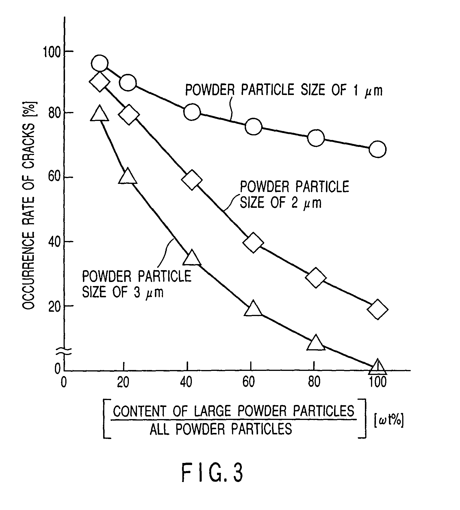
[0097]For example, an Ni powder having an average particle size of 1 μm is dispersed in a methanol solution, and the solution is applied to a substrate in which a plug is formed. Since the dispersed NI powder precipitates, the Ni powder is deposited on the substrate. The substrate is then dried to evaporate the methanol. Thereafter, the Ni powder is calcined. As a consequence, the powder is completely buried in the trench (this method will be referred to as the precipitation method hereinafter). After this process, the Ni powder portion calcined outs...


PUM

PropertyMeasurementUnit
viscositiesaaaaaaaaaa
particle sizeaaaaaaaaaa

Abstract

Form a trench in a major surface of a semiconductor substrate, then bury a paste in the trench. The paste contains solids having a conductive substance and a resin, and solvent for dissolving the resin. The solids content of the paste is not less than 60 vol % and a viscosity ratio thereof is not more than 2.

Description

[0001]This is a divisional of application Ser. No. 09 / 722,467, filed Nov. 28, 2000, now U.S. Pat. No. 6,657,306, which is a divisional of application Ser. No. 09 / 321,534, filed May 28, 1999, now U.S. Pat. No. 6,235,624, and claims the benefit of Japanese Application no. 10-258830, filed Sep. 11, 1998, all of which are incorporated herein by reference.BACKGROUND OF THE INVENTION[0002]To improve the performance and, particularly, speed of an electronic circuit system constituted by a plurality of semiconductor chips, it has become increasingly important to reduce the length of the interconnections between the semiconductor chips to a minimum.[0003]For this purpose, a technique of minimizing the interconnections between a plurality of semiconductor chips by stacking them has been studied instead of the conventional method of mounting a plurality of semiconductor chips two-dimensionally on a multilayer board. Such a semiconductor device formed by stacking a plurality of semiconductor ch...

Claims


Application Information

Patent Timeline
Patent Type & Authority Patents(United States)
IPC IPC(8): H01L21/4763H01L21/44H01L21/288H01L21/768H01L23/48
CPCH01L21/288H01L21/76877H01L21/76882H01L21/76898H01L23/481H01L2924/0002Y10S438/977H01L2924/00
Inventor SASAKI, KEIICHIKIMURA, MANABUHISATSUNE, YOSHIMIHAYASAKA, NOBUO
Owner KK TOSHIBA
Why Eureka
Try Eureka