Photonic device with segmented absorption design

a photonic device and segmented absorption technology, applied in the field of optoelectronic components, can solve the problems of affecting the reliability of long-term devices, and local increase of the absorption coefficient of semiconductor materials, so as to reduce the maximum local temperature and optimize heat dissipation

Active Publication Date: 2006-05-23
LUMENTUM OPERATIONS LLC
View PDF5 Cites 14 Cited by
  • Summary
  • Abstract
  • Description
  • Claims
  • Application Information

AI Technical Summary

Benefits of technology

[0013]A photonic device designed with an intermittent absorption profile along a waveguide. The absorption profile is divided into low-absorption and high-absorption segments that are distributed axially in order to decrease the maximum local temperature in the device. The d

Problems solved by technology

Strong heating at the front of the device will cause a local increase of the absorption coefficient of the semiconductor material due to bandgap shrinkage.
[3] This feedback cycle can cause a thermal runaway, resulting in a catastrophic device failure.
[4] Even if the device does not fail i

Method used


Image

  • Photonic device with segmented absorption design
  • Photonic device with segmented absorption design
  • Photonic device with segmented absorption design

Examples


Embodiment Construction

[0026]In the following description of the preferred embodiment, reference is made to the accompanying drawings which form a part hereof, and in which is shown by way of illustration a specific embodiment in which the invention may be practiced. It is to be understood that other embodiments may be utilized and structural changes may be made without departing from the scope of the present invention.

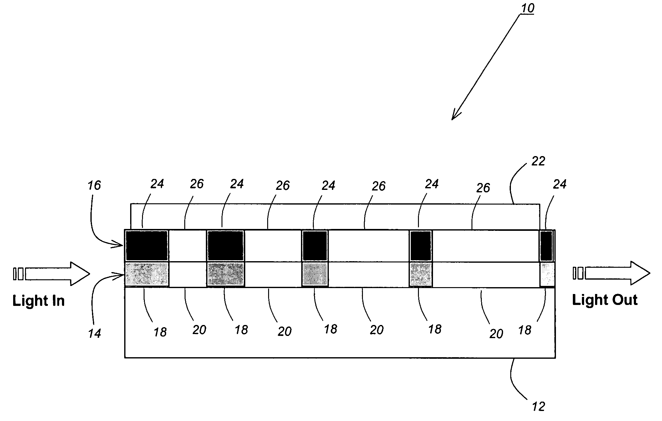
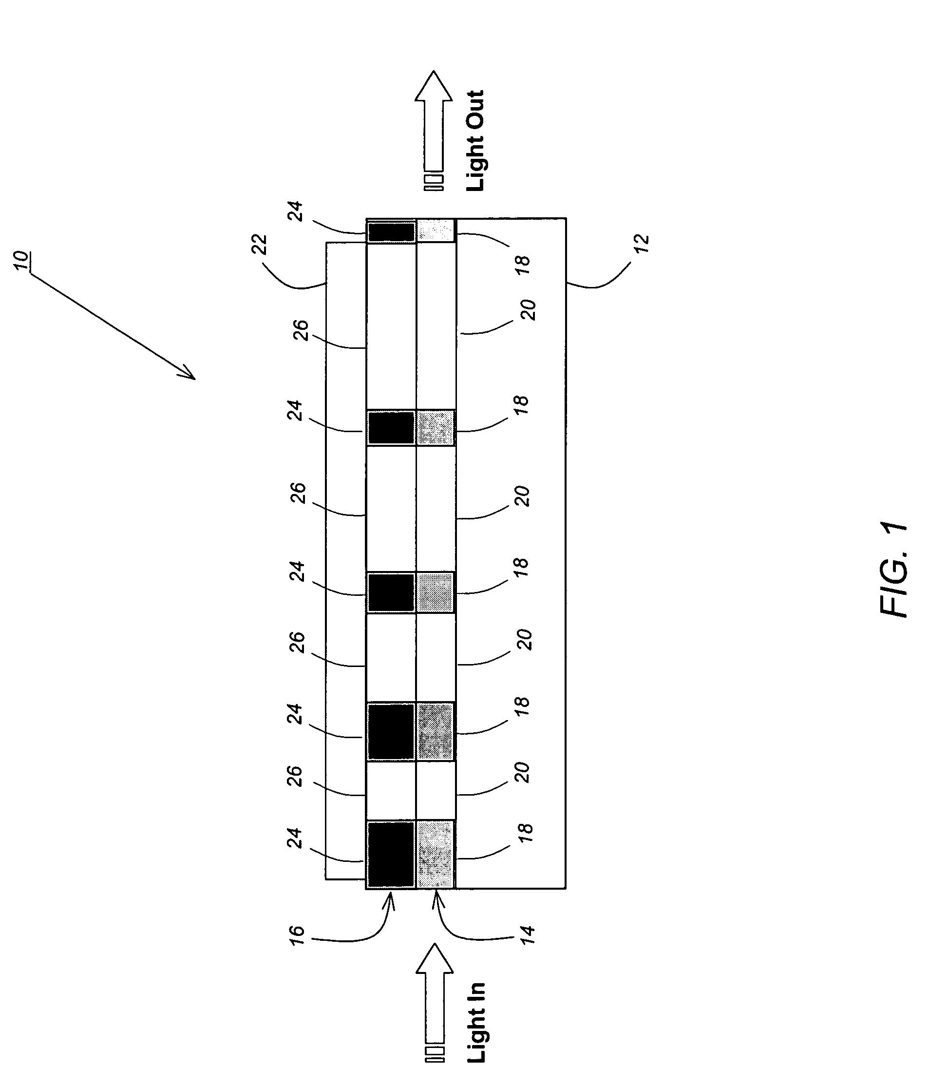
[0027]In the present invention, the total light absorption of a waveguide optical element is spread axially through the use of segments in which the absorption coefficient alternates between a large and a small value. Light absorption, and therefore generated photocurrent, is high in segments with a large absorption coefficient. By inserting low-absorption or non-absorption segments, the heat generated by the photocurrent is allowed to dissipate in a more efficient manner, reducing the overall temperature of the device and the degree of temperature non-uniformity.

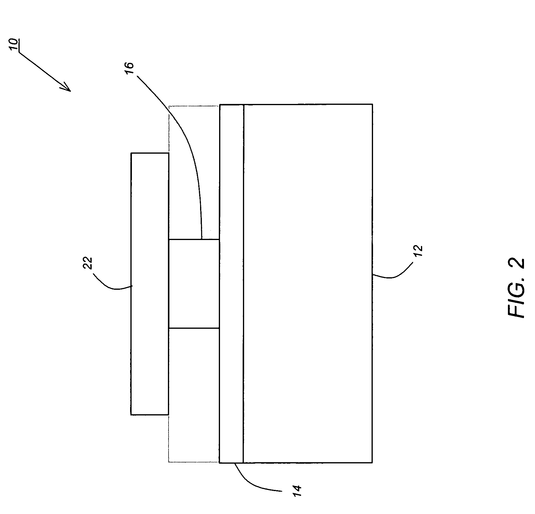
[0028]FIGS. 1, 2, and 3 sho...


PUM


Abstract

A photonic device designed with an intermittent absorption profile along a waveguide. The absorption profile is divided into low-absorption and high-absorption segments that are distributed axially in order to decrease the maximum local temperature in the device. The distribution of low-absorption segments can be controlled through techniques such as proton implantation or selective-area quantum well intermixing. The lengths of low-absorption and high-absorption segments can be adjusted to optimize heat dissipation along the device length.

Description

CROSS-REFERENCE TO RELATED APPLICATIONS[0001]This application claims the benefit under 35 U.S.C. §119(e) of co-pending and commonly-assigned U.S. provisional patent application Ser. No. 60 / 429,132, filed Nov. 26, 2002, by Torsten Wipiejewski, and entitled “ELECTRO-ABSORPTION MODULATOR WITH SEGMENTED ABSORPTION DESIGN,” which application is incorporated by reference herein.BACKGROUND OF THE INVENTION[0002]1. Field of the Invention[0003]This invention relates to optoelectronic components, and more particularly, to a waveguide-based optically absorbing device.[0004]2. Description of the Related Art[0005](Note: This application references a number of different patents, applications and / or publications as indicated throughout the specification by reference numbers enclosed in brackets, e.g., [x]. A list of these different patents, applications and / or publications ordered according to these reference numbers can be found below in the section entitled “References.” Each of these patents, a...

Claims


Application Information

Patent Timeline
IPC IPC(8): G02B6/10G02B6/12G02B6/122G02F1/025G02F1/225
CPCG02B6/122G02F1/025G02F1/2257G02B2006/12159
Inventor WIPIEJEWSKI, TORSTENKOZODOY, PETER
Owner LUMENTUM OPERATIONS LLC
Why Eureka
Try Eureka