
Microchip, method of manufacturing microchip, and method of detecting compositions

a microchip and composition technology, applied in the field of microchips, can solve the problems of complex manufacturing methods and inability to measure the concentration of samples flowing through the channel in high precision, and achieve the effect of high precision

Inactive Publication Date: 2006-06-06
NEC CORP
View PDF21 Cites 13 Cited by
  • Summary
  • Abstract
  • Description
  • Claims
  • Application Information

AI Technical Summary

Benefits of technology

[0010]An object of the present invention is to provide a technique with which a sample flowing in a channel can be analyzed in high precision even in a microchip having a fine structure.
[0011]Another object of the present invention is to provide a technique with which compositions of a sample can be detected optically even in a very small channel formed on a plane.
[0012]Still another object of the present invention is to provide a technique with which a sufficient long optical length can be secured even in a shallow channel, and compositions of a sample flowing in the channel can be detected in high precision.

Problems solved by technology

As a result, there is such a risk that the concentration of the sample flowing through the channel cannot be measured in high precision.
Thus, a method of manufacturing it becomes complex.

Method used


Image

  • Microchip, method of manufacturing microchip, and method of detecting compositions
  • Microchip, method of manufacturing microchip, and method of detecting compositions
  • Microchip, method of manufacturing microchip, and method of detecting compositions

Examples


first embodiment

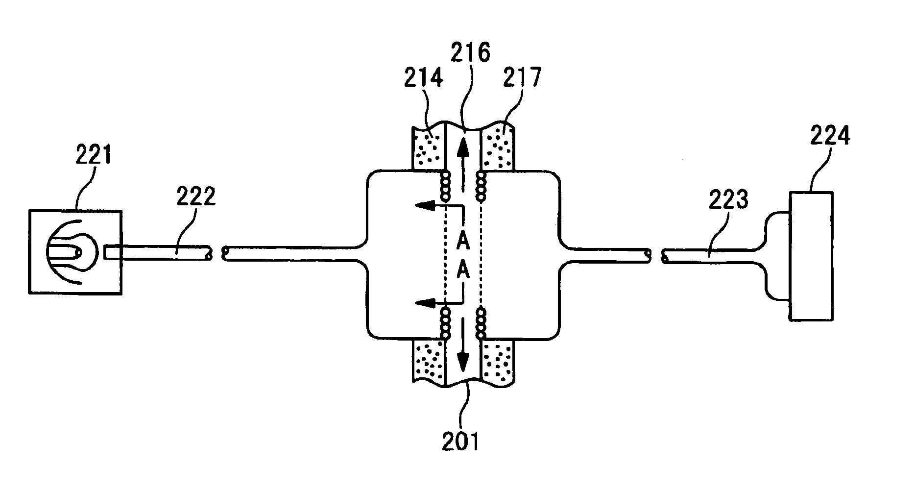
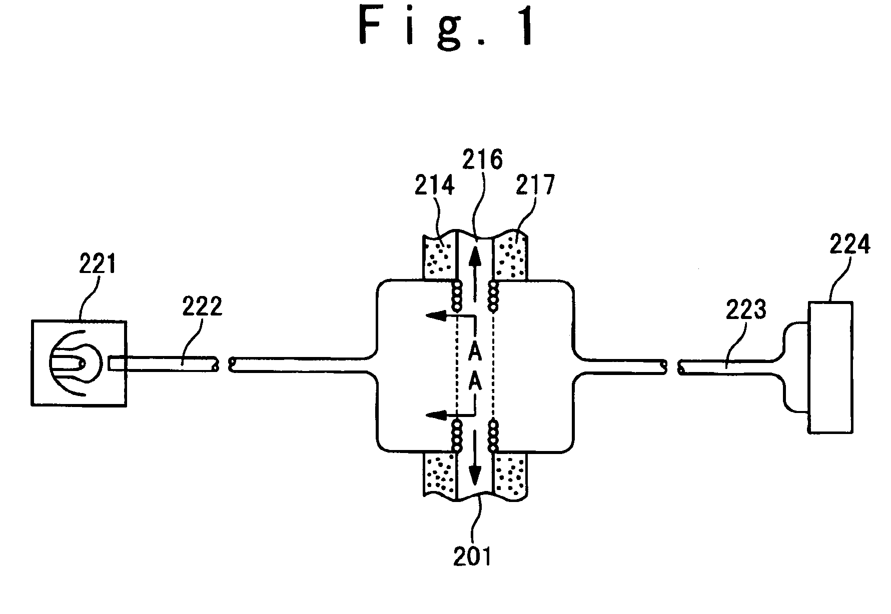
[0082]FIGS. 3A to 3C are diagrams showing structures of a microchip according to a first embodiment of the present invention. The microchip 10 according to the present embodiment has a function capable of separating compositions contained in a sample. FIG. 3A is a top view of the microchip 10. The microchip 10 is provided with a liquid reservoir 22a, a liquid reservoir 22b, a liquid reservoir 23, a liquid reservoir 24, a liquid reservoir 25a, and a liquid reservoir 25b. Also, a light leading optical fiber 42a is connected via an optical connector 40a to the microchip 10, and a light receiving optical fiber 42b is connected via an optical connector 40b to the microchip 10.

[0083]FIG. 3B is a cross sectional view of the microchip along A–A′ in FIG. 3A. The microchip 10 has a substrate 12 and a cover member 20. The substrate 12 includes a lower clad layer 14, and an upper clad layer 18 which is provided on the lower clad layer 14. A light leading optical waveguide 32a and a light receiv...

second embodiment

[0112]FIG. 5 is a cross sectional view showing a structure of a microchip according to a second embodiment of the present invention. In the present embodiment, the same reference numerals in the first embodiment shown in FIG. 3C are given to the same components, and explanations thereof are properly omitted.

[0113]When a light which is transmitted from the external light source via the light leading optical waveguide 32a is entered to the separation channel 28, the entered light is broadened and scattered within the separation channel 28. In this case, an amount of light which is transmitted to the light receiving optical waveguide 32b is decreased. Therefore, according to the present embodiment, the light leading optical waveguide 32a and the light receiving optical waveguide 32b are formed in such a manner that these optical waveguides 32a and 32b have wide width portions at boundaries with respect to the separation channel 28. The wide width portions are made wider than the other ...

third embodiment

[0115]FIG. 6A is a schematic diagram for showing a microchip according to a third embodiment of the present invention. FIG. 6B is a cross sectional view showing the microchip in FIG. 6A. In the present embodiment, the same reference numerals in the first embodiment shown in FIGS. 3A and 3C are given to the same components, and explanations thereof are properly omitted.

[0116]According to the present embodiment, a microchip 52 is different from the first embodiment in that the microchip 52 has not only a combination of a light leading optical waveguide 32a and a light receiving optical waveguide 32b but also a combination of a light leading optical waveguide 34a and a light receiving optical waveguide 34b. The light leading optical waveguide 32a and the light receiving optical waveguide 32b are provided opposite to each other on both sides of the separation channel 28. Also, the light leading optical waveguide 34a and the light receiving optical waveguide 34b are provided opposite to ...


PUM

PropertyMeasurementUnit
widthaaaaaaaaaa
depthaaaaaaaaaa
depthaaaaaaaaaa

Abstract

A microchip includes a clad layer having a channel through which a sample flows, and an optical waveguide formed within the clad layer and having a higher refractive index than the clad layer. The optical waveguide is formed to act on the channel optically. Thus, the sample flowing in the channel can be analyzed with high accuracy even in the microchip having a fine structure.

Description

[0001]This is a continuation of Application Ser. No PCT / JP03 / 09720, filed Jul. 31, 2003.TECHNICAL FIELD[0002]The present invention relates to a microchip, a method of manufacturing the microchip, and a method of detecting compositions.BACKGROUND ART[0003]There are strong needs for a microchip in a clinical investigation and a proteomics analysis. The microchip is used to separate biomolecule such as nucleic acid and protein and to analyze the separated sample. In such an analysis of the sample, a method for optically detecting very small amounts of separated samples has been utilized. As a technique for optically analyzing the samples, a transmission light technique and a diffuse reflection technique are known.[0004]According to the diffuse reflection technique, a sample is analyzed by detecting a reflected light of a laser light which is irradiated to the sample. A densitometry apparatus described in Japanese Laid-open Patent Application No. 2002-98637 employs a laser emitting devi...

Claims


Application Information

Patent Timeline
Patent Type & Authority Patents(United States)
IPC IPC(8): G02B6/00H01L21/00G01N33/483B01L3/00G01N21/05G01N21/27G01N21/33G01N37/00G01Q60/22
CPCB01L3/502715G01N21/05B01L2300/0654B01L2300/0816G01N2021/0346B01L2300/168B01L2300/0887
Inventor IIDA, KAZUHIROTOKUSHIMA, MASATOSHISHIMODA, TSUYOSHI
Owner NEC CORP
Learn More