
Structure of image sensor module and a method for manufacturing of wafer level package

a technology of image sensor module and manufacturing method, which is applied in the direction of television system, radio frequency controlled devices, printed circuit non-printed electric components association, etc., can solve the problems of reducing yield, reducing package technology, and reducing the yield of frame package technology, so as to facilitate the final testing of wafer level package, reduce the cost of package structure, and increase the yield of package structure

Active Publication Date: 2006-06-13
ADL ENERGY CORP
View PDF6 Cites 56 Cited by
  • Summary
  • Abstract
  • Description
  • Claims
  • Application Information

AI Technical Summary

Benefits of technology

This approach lowers packaging costs, increases yield, and enhances reliability by simplifying the manufacturing process, improving thermal conductivity, and allowing for efficient signal transmission, making it suitable for both semiconductor and LCD industries.

Problems solved by technology

It causes the packaging for the semiconductor dies to become more difficult and decrease the yield.
The earlier lead frame package technology is already not suitable for the advanced semiconductor dies due to the density of the pins thereof is too high.
The one drawback of the method of the COB is lower yield rate during packaging process due to particle contamination on sensing area.
Besides, the drawbacks of the method of the LCC are higher packaging cost due to materials and lower yield rate during packaging process due to particle contamination on sensing area.
Moreover, SHELL CASE company also develops wafer level package technique, the image sensor dies packaged by the SHELL CASE is higher cost due to requiring two glass plate and complicate process.
And, the transparency is bad due to epoxy wearing out, and the potential reliability may be reduced.

Method used


Image

  • Structure of image sensor module and a method for manufacturing of wafer level package
  • Structure of image sensor module and a method for manufacturing of wafer level package
  • Structure of image sensor module and a method for manufacturing of wafer level package

Examples


Embodiment Construction

[0024]Some sample embodiments of the invention will now be described in greater detail. Nevertheless, it should be recognized that the present invention can be practiced in a wide range of other embodiments besides those explicitly described, and the scope of the present invention is expressly not limited expect as specified in the accompanying claims.

[0025]Then, the components of the different elements are not shown to scale. Some dimensions of the related components are exaggerated and meaningless portions are not drawn to provide a more clear description and comprehension of the present invention.

[0026]The die of the present invention may be packaged with passive components (ex. capacitors) or other dies with a side by side structure or a stacking structure. The IC package can be finished by semiconductor industry and LCD industry.

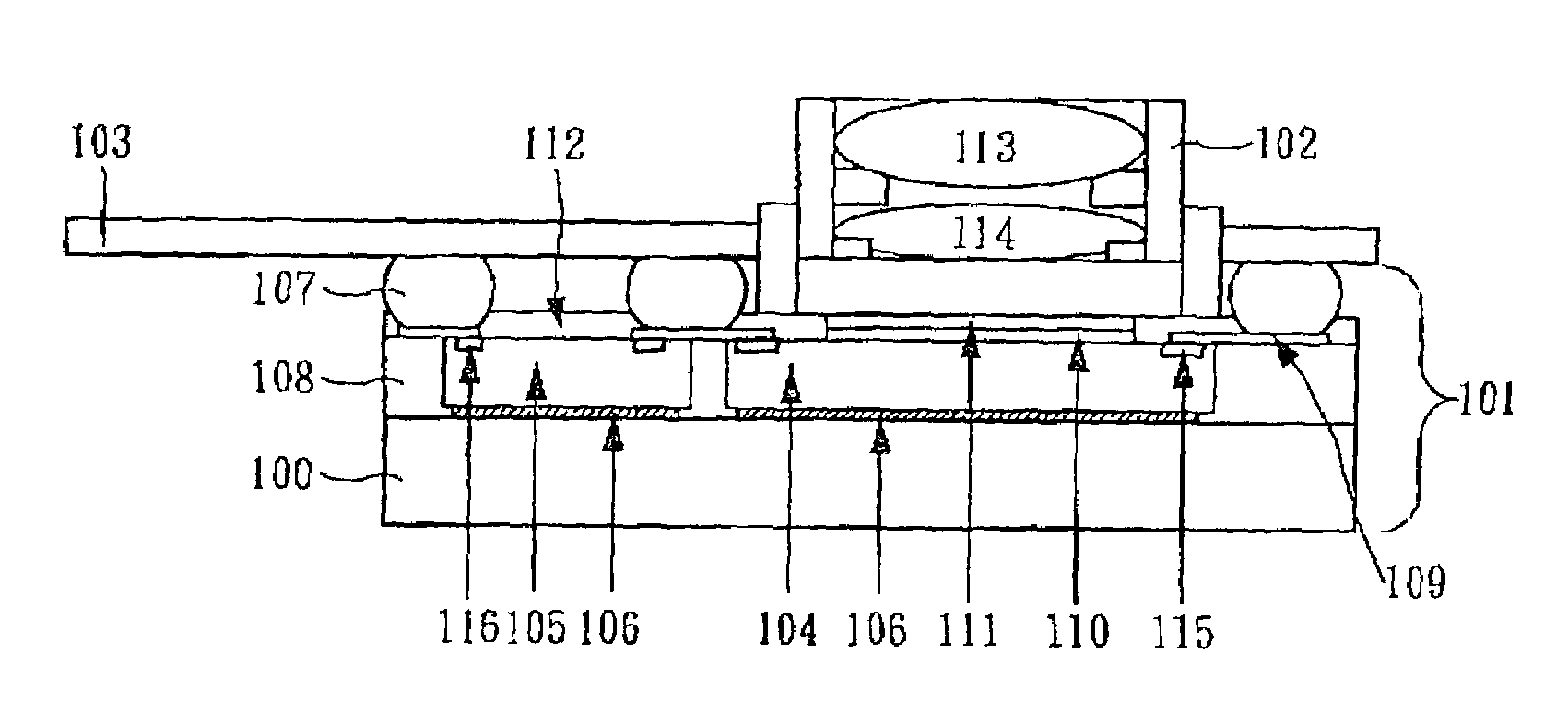
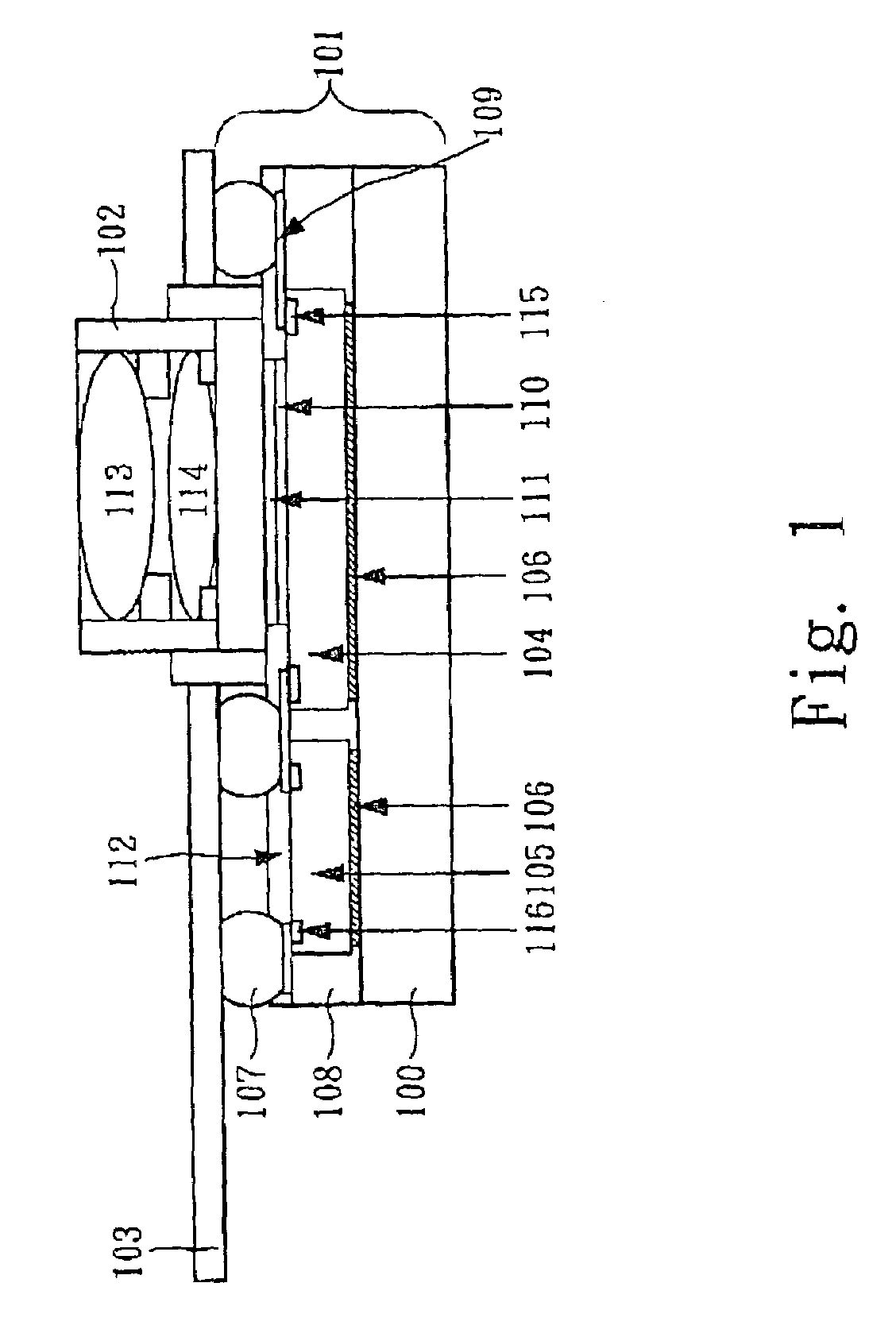
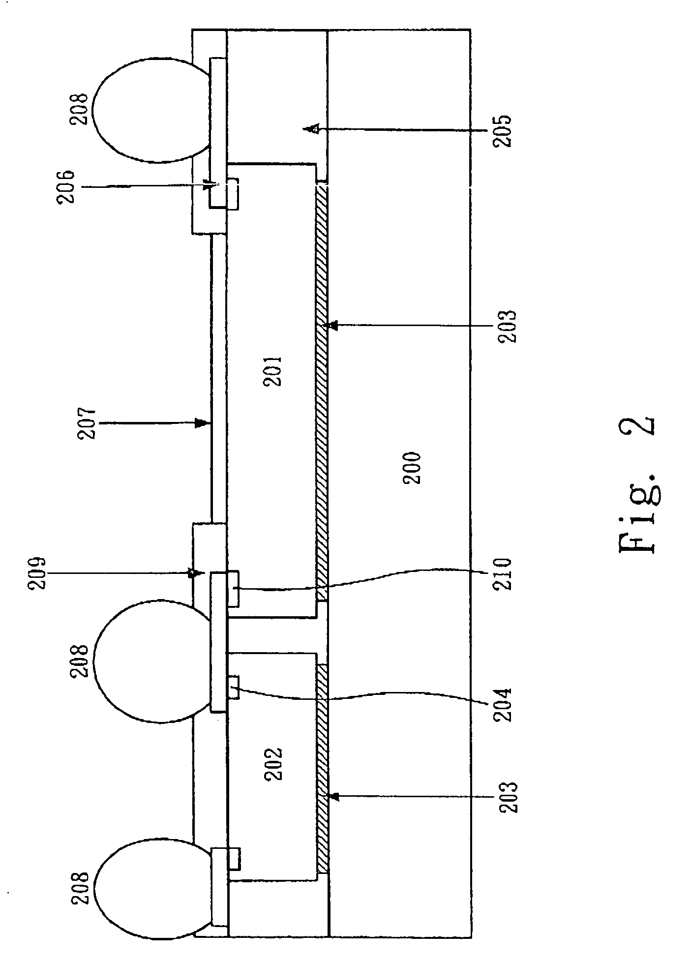
[0027]As aforementioned, the present invention provides an image sensor module, as shown in FIG. 1. The cross-section of the wafer level package struct...


PUM


Abstract

The present invention discloses an image sensor module and forming method of wafer level package. The image sensor module comprises an isolating base, a wafer level package, a lens holder, and a F.P.C.. The wafer level package having a plurality of image sensor dies and a plurality of solder balls is attached to the isolating base. A plurality of lens are placed in the lens holder, and the lens holder is located on the image sensor dies. The lens holder is placed in the F.P.C., and the F.P.C. has a plurality of solder joints coupled to the solder balls for conveniently transmitting signal of the image sensor dies. Moreover, the image sensor dies may be packaged with passive components or other dies with a side by side structure or a stacking structure.

Description

BACKGROUND OF THE INVENTION[0001]1. Field of the Invention[0002]This invention relates to an image sensor module, and more particularly to an image sensor module and a structure and method for manufacturing of wafer level package that can lower the cost, raise the yield and reliability.[0003]2. Description of the Prior Art[0004]The semiconductor technologies are developing very fast, and especially semiconductor dies have a tendency toward miniaturization. However, the requirements for the functions of the semiconductor dies have an opposite tendency to variety. Namely, the semiconductor dies must have more I / O pads into a smaller area, so the density of the pins is raised quickly. It causes the packaging for the semiconductor dies to become more difficult and decrease the yield.[0005]The main purpose of the package structure is to protect the dies from outside damages. Furthermore, the heat generated by the dies must be diffused efficiently through the package structure to ensure t...

Claims


Application Information

Patent Timeline
Patent Type & Authority Patents(United States)
IPC IPC(8): H01L23/34H01L27/14H01L21/00H01L21/50H01L21/56H01L23/12H01L23/50H01L27/144H01L27/146H01L29/06H01L31/00H01L31/0203H01L31/0232H01L31/10H04N5/225H05K1/18
CPCH01L27/14618H01L27/14627H01L27/14632H01L27/14685H01L27/14687H01L31/0203H01L31/0232H01L24/97H01L21/561H01L2224/97H01L2224/92244H01L2224/73267H01L2224/32225H01L2224/32145H01L27/14625H01L2224/04105H01L2224/20H01L2224/211H01L2924/01077H01L2924/01078H01L2924/01079H01L2924/09701H01L2924/15311H05K1/189H01L2924/01068H01L2924/10253H01L2224/24137H01L2924/00H01L2224/83H01L2224/82H01L2924/15788H01L2924/14H01L31/02325H01L2224/83874H01L2224/12105H01L27/146H01L31/10
Inventor YANG, WEN-KUNYANG, WEN-PIN
Owner ADL ENERGY CORP
Learn More