

Data path having grounded precharge operation and test compression capability
a data path and pre-charge operation technology, applied in the field of data paths in memory devices, can solve the problems of line impedances and negatively affecting the write tim
- Summary
- Abstract
- Description
- Claims
- Application Information
AI Technical Summary
Benefits of technology
Problems solved by technology
Method used
Image

Examples
Embodiment Construction
[0020]Certain details are set forth below to provide a sufficient understanding of the invention. However, it will be clear to one skilled in the art that the invention may be practiced without these particular details. In other instances, well-known circuits, control signals, timing protocols, and software operations have not been shown in detail in order to avoid unnecessarily obscuring the invention.
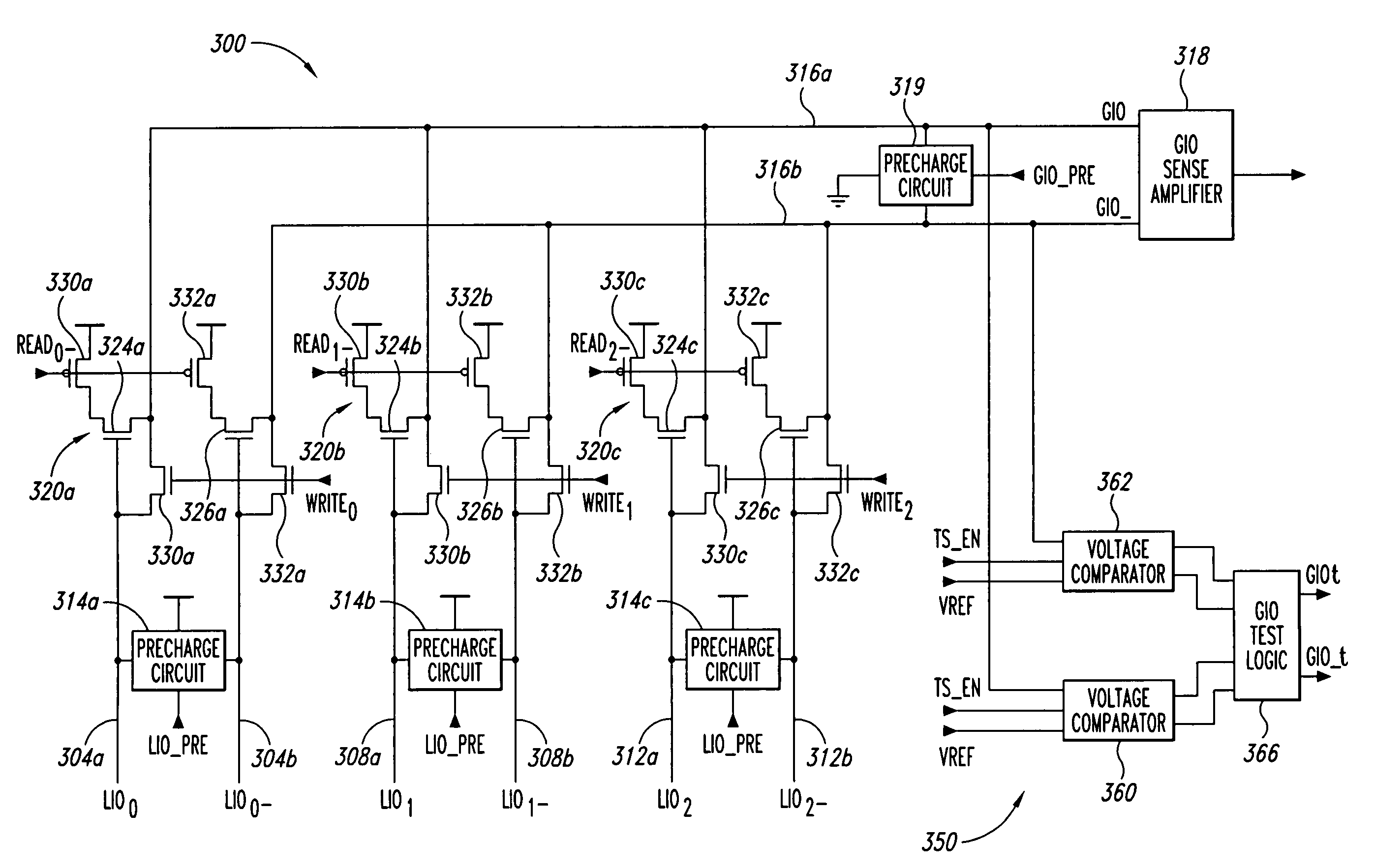
[0021]FIG. 3 illustrates a data path 300 according to an embodiment of the present invention. The data path 300 includes three local input / output (LIO) lines 304, 308, 312 coupled to a global input / output (GIO) line 316. It will be appreciated by those ordinarily skilled in the art that greater or fewer LIO lines can be coupled to the GIO line 316 without departing from the scope of the present invention. The LIO lines 304, 308, 312 are shown in FIG. 3 for merely the purpose of providing an example. Each of the LIO lines 304, 308, 312 is formed from a pair of respective signals lines ...
PUM
 Abstract
Description
Claims
Application Information