Bundled probe apparatus for multiple terminal contacting

a probe apparatus and probe technology, applied in the direction of resistance/reactance/impedence, instruments, measurement devices, etc., can solve the problems of increasing the difficulty of removing oxide layers, the time is not enough to establish sufficient contact quality between the probe and the chip terminal, and the voltage level at which the circuit chips opera

Inactive Publication Date: 2006-06-20
INTERCONNECT DEVICES
View PDF21 Cites 45 Cited by
  • Summary
  • Abstract
  • Description
  • Claims
  • Application Information

AI Technical Summary

Problems solved by technology

The continuing development of circuit chips results in an ever decreasing voltage level at which the circuit chips operate and have to be tested.
On the other hand, the chip testing has to be performed with shortest possible testing times, leaving little time for establishing sufficient contacting quality between the probes and the chip terminals.
As a result, the removal of oxide layers becomes more difficult to accomplish.

Method used


Image

  • Bundled probe apparatus for multiple terminal contacting
  • Bundled probe apparatus for multiple terminal contacting
  • Bundled probe apparatus for multiple terminal contacting

Examples


first embodiment

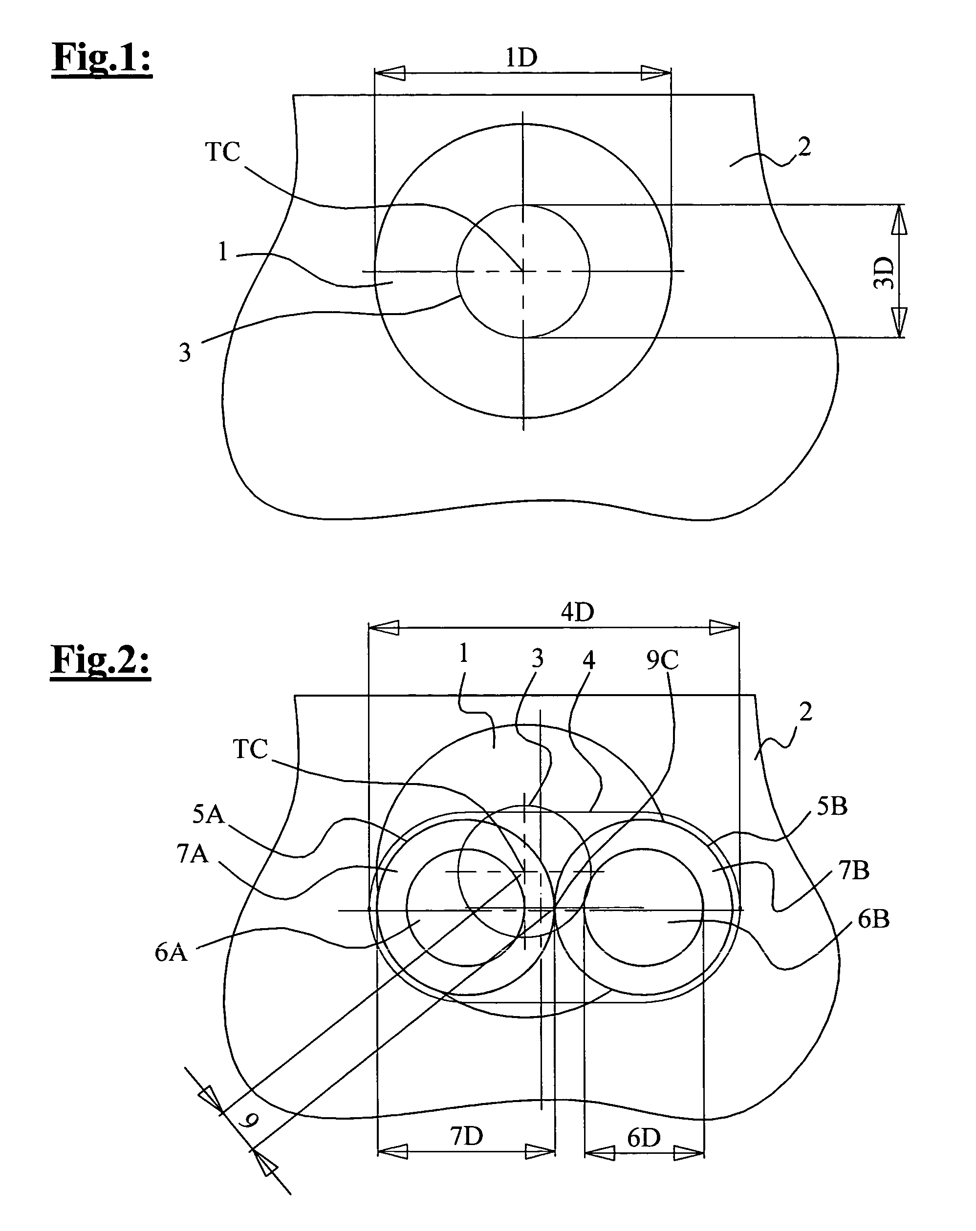
[0027]FIG. 2 shows a top view of the terminal 1 being contacted by first and second probes 5A, 5B according to the invention. First and second probes 5A, 5B have a common contacting center 9C, which is shown in a position within the probe target area 3. For the sole purpose of general understanding, the common contacting center 9C is shown in an offset distance 9 relative to the terminal center TC, which is also the center of the probe target area 3. It is clear that the common contacting center 9C may be positioned at any location within the probe target area 3 during a real life testing.

[0028]First and second probes 5A, 5B are exemplarily shown as being essentially cylindrical and protruding in view direction. The first and second probes 5A, 5B represent in a simplified form buckling beam probes as are well known to those skilled in the art. It is noted that the scope of the invention is not limited to buckling beam probes having circular section shapes in their portions dedicated...

second embodiment

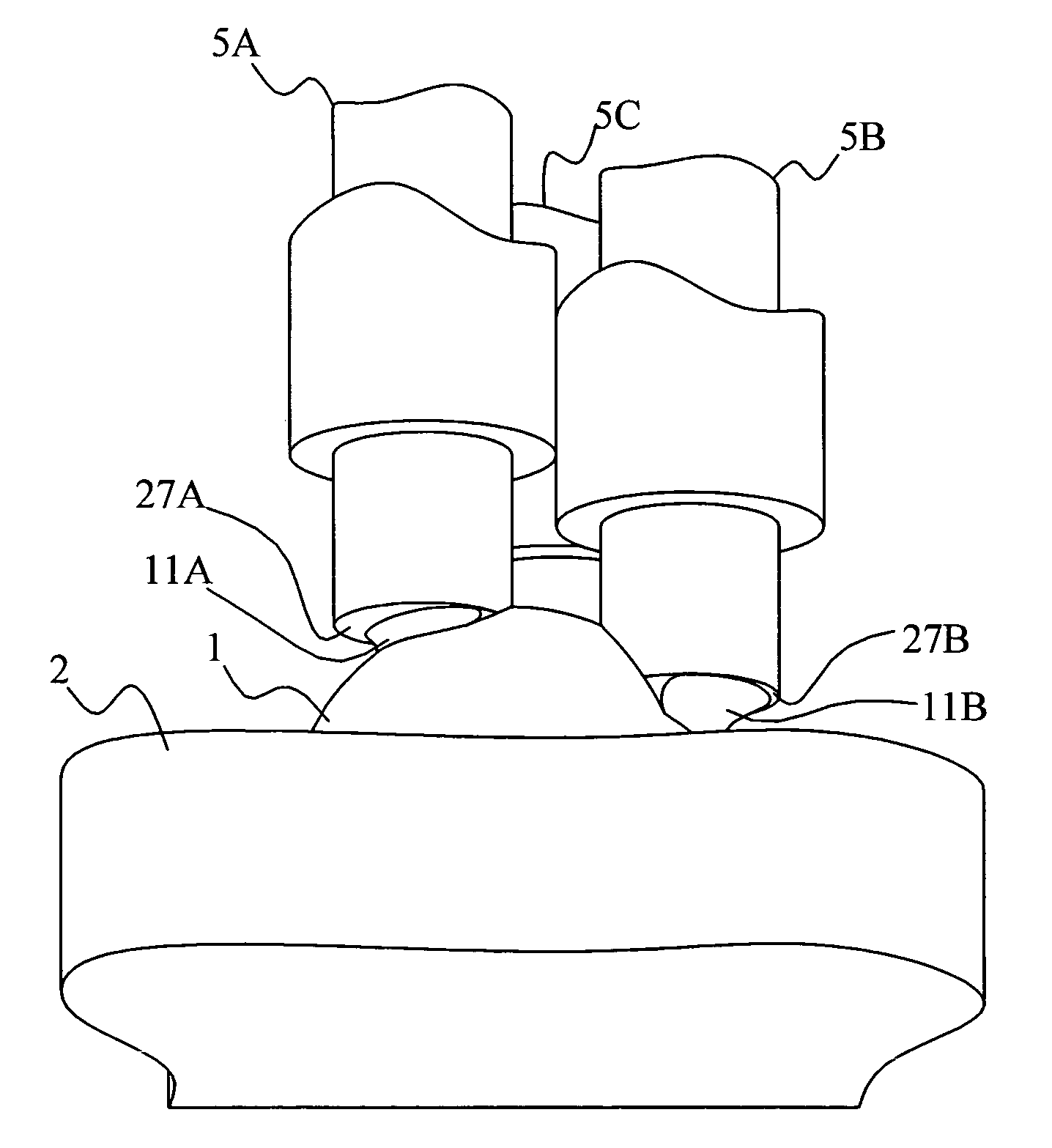
[0036]FIG. 4 shows a top view of the invention in which three probes 5A, 5B, 5C are combined in a probe group dedicated for contacting the single terminal 1. The third probe 5C preferably conforms in its configuration to the first and second probes 5A, 5B.

[0037]The teachings stated for the first embodiment may be applied to the second embodiment with following differences:[0038]1. The presence of three probes 5A, 5B, 5C provides for three individual path resistances rather than only one path resistance as described for the first embodiment. A first path resistance is provided along first and second probe 5A, 5B, the terminal 1 and the corresponding interfaces. A second path resistance is provided along first and third probe 5A, 5C, the terminal 1 and the corresponding interfaces. A third path resistance is provided along second and third probe 5B, 5C, the terminal 1 and the corresponding interfaces. The three path resistances have a constant resistance portion and a variable resista...


PUM


Abstract

A probe apparatus having probe groups comprising two or three probes that independently contact single terminals of tested chips. As a result, the probe apparatus is capable of recognizing voltage drops of a test signal applied prior to the chip testing onto a test path along two or three probes contacting, the terminal and the interfaces between them. The test path does not pass through the chip. An electronic circuit measures the voltage drops and compensated accordingly operational signals passing through the terminals, the probes and the interfaces during the chip testing. A first embodiment comprises two probes per group. A second embodiment comprises three probes per group. In the second embodiment, the variable resistance component of three resistance measurements of first / second, first / third and second / third resistance paths are compared by the electronic circuit, in order to determine absolute resistance values for each of the three signal paths. Consequently, in the second embodiment, the voltage drops may be individually adjusted for each of the three operational signal paths.

Description

FIELD OF INVENTION[0001]The invention relates to probe apparatus for testing electronic circuit chips. Particularly, the present invention relates to a probe apparatus capable of recognizing and compensating resistance discrepancies in contact interfaces between chip terminals and probe tips.BACKGROUND OF INVENTION[0002]Before electronic circuit chips are packaged, they are conventionally tested to retrieve information about their performance levels. A performance criterion, for example, are voltage level discrepancies within the tested chip. The continuing development of circuit chips results in an ever decreasing voltage level at which the circuit chips operate and have to be tested. The recognition of voltage level discrepancies at ever decreasing operational voltage levels requires more precise inducing and deriving of test signals during the chip testing. For a cost effective chip fabrication it is at the same time desirable to have a probe apparatus capable of compensating for...

Claims


Application Information

Patent Timeline
Patent Type & Authority Patents(United States)
IPC IPC(8): G01R27/08G01R1/067G01R1/073G01R31/28
CPCG01R1/06794G01R1/07307G01R31/2886
Inventor KISTER, JANUARYDABROWIECKI, KRZYSZTOF
Owner INTERCONNECT DEVICES
Why Eureka
Try Eureka