Exposure apparatus and method

a technology of exposure apparatus and light source, which is applied in the field of nmorder micropatterning for semiconductors, can solve the problems of limited light source, and limited conventional projection exposure apparatus, and achieve the effect of shortening the exposure tim

Inactive Publication Date: 2006-06-27
CANON KK
View PDF9 Cites 7 Cited by
  • Summary
  • Abstract
  • Description
  • Claims
  • Application Information

AI Technical Summary

Benefits of technology

[0005]The present invention has been made to overcome the conventional drawbacks, and has as its first object to provide an exposure apparatus and a method capable of realizing processing at a resolving power corresponding to a wavelength shorter than the wavelength of a light source, and shortening the exposure time.

Problems solved by technology

In general, a conventional projection exposure apparatus is limited in micropatterning by the wavelength of a light source.
Thus, the apparatus is limited in light quantity to be obtained and in shortening the exposure time.
An exposure apparatus and a method using a near-field formed by such a small opening are difficult to bring a plurality of openings close to each other and perform exposure independently through these openings.

Method used


Image

  • Exposure apparatus and method
  • Exposure apparatus and method
  • Exposure apparatus and method

Examples


Embodiment Construction

[0039]Preferred embodiments of the present invention will now be described in detail in accordance with the accompanying drawings.

[0040]An exposure apparatus according to a preferred embodiment of the present invention is used to process a small region by irradiating a photosensitive material in the small region with light. That is, a pattern is formed by irradiating with light a photosensitive material which chemically, physically changes by irradiation of light. For example, this exposure apparatus is employed when a resist applied to a semiconductor surface is irradiated to form a pattern.

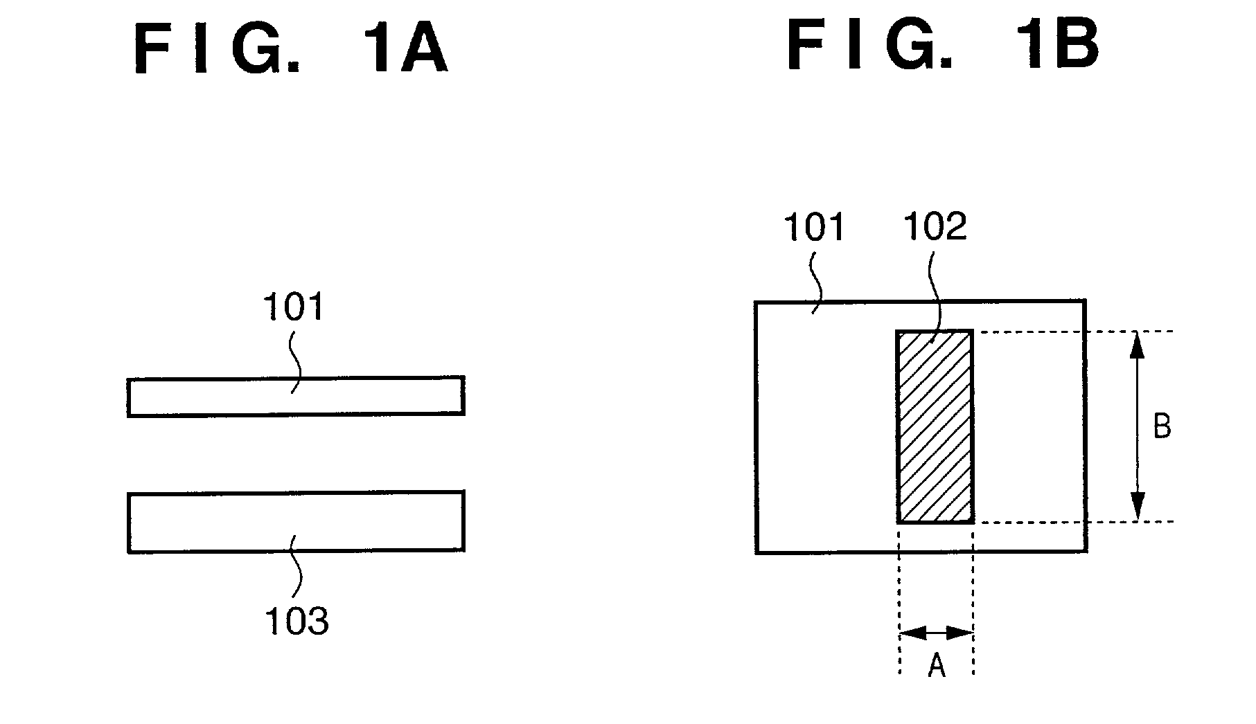
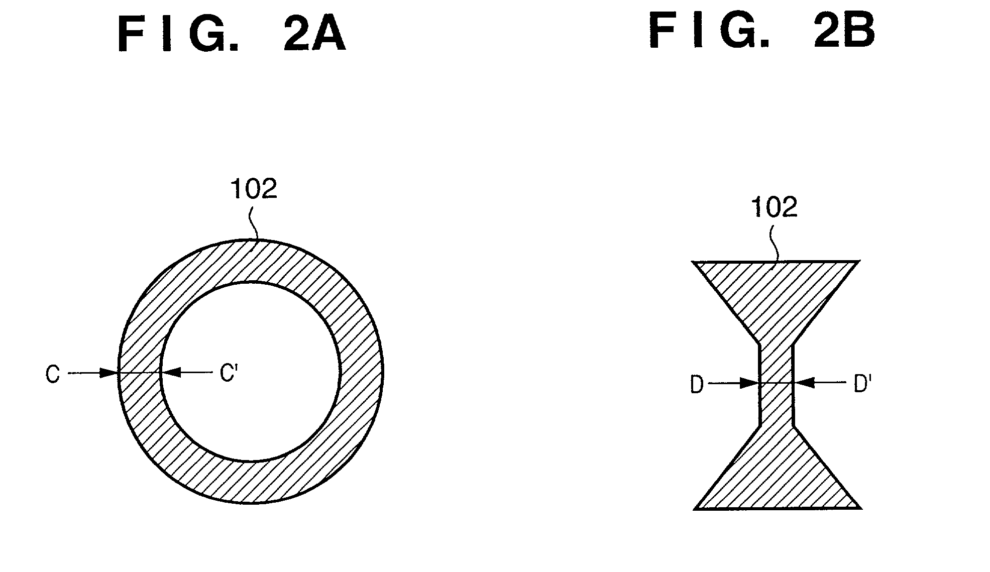
[0041]At least part of a light-emitting portion in this embodiment is smaller in width than the wavelength. The width of the light-emitting portion means one when viewed from a plane facing a photosensitive member to be exposed.

[0042]FIGS. 1A and 1B are views for explaining a light-emitting portion according to the embodiment of the present invention. FIG. 1A is a sectional view when a plate-lik...


PUM

PropertyMeasurementUnit
diameteraaaaaaaaaa
diameteraaaaaaaaaa
widthaaaaaaaaaa

Abstract

An exposure apparatus includes a light-emitting portion arranged so as to be opposite to a photosensitive member at a position for exposure. A part of the light-emitting portion is smaller in width than a wavelength of light from the light-emitting portion.

Description

FIELD OF THE INVENTION[0001]The present invention relates to nm-order micropatterning for semiconductors and the like.BACKGROUND OF THE INVENTION[0002]Recent advances of semiconductor micropatterning techniques enable processing at the 100 [nm] level. Along with this, the integration degree is increasing, and new devices using the quantum effect, or the like, are being manufactured. For example, Japanese Patent Laid-Open No. 11-145051 discloses an exposure method using near-field light. In general, a conventional projection exposure apparatus is limited in micropatterning by the wavelength of a light source. However, an exposure apparatus using near-field light realizes processing of a light wavelength or less.[0003]A conventionally-disclosed micropatterning apparatus using near-field light adopts an opening smaller than the wavelength of a light source, and utilizes a near-field formed by the opening. Thus, the apparatus is limited in light quantity to be obtained and in shortening...

Claims


Application Information

Patent Timeline
Patent Type & Authority Patents(United States)
IPC IPC(8): G03B27/54B82B1/00G03B27/42G03F7/20H01L21/027
CPCG03F7/70058G03B27/42
Inventor YANO, KOJIKURODA, RYOOKAMOTO, KOHEI
Owner CANON KK
Why Eureka
Try Eureka