IC substrate of glass and display device

Inactive Publication Date: 2006-07-04
SANYO ELECTRIC CO LTD
View PDF16 Cites 38 Cited by
  • Summary
  • Abstract
  • Description
  • Claims
  • Application Information

AI Technical Summary

Benefits of technology

[0010]Accordingly, this invention intends to

Problems solved by technology

In addition, the semiconductor wafer having a large size is generally expensive.
This is an obstacle to reduce the production cost.
Therefore

Method used


Image

  • IC substrate of glass and display device
  • IC substrate of glass and display device
  • IC substrate of glass and display device

Examples


Embodiment Construction

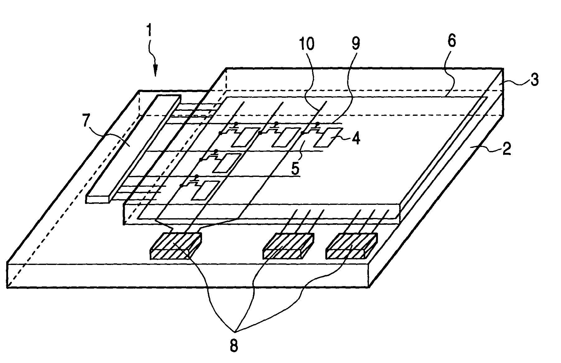
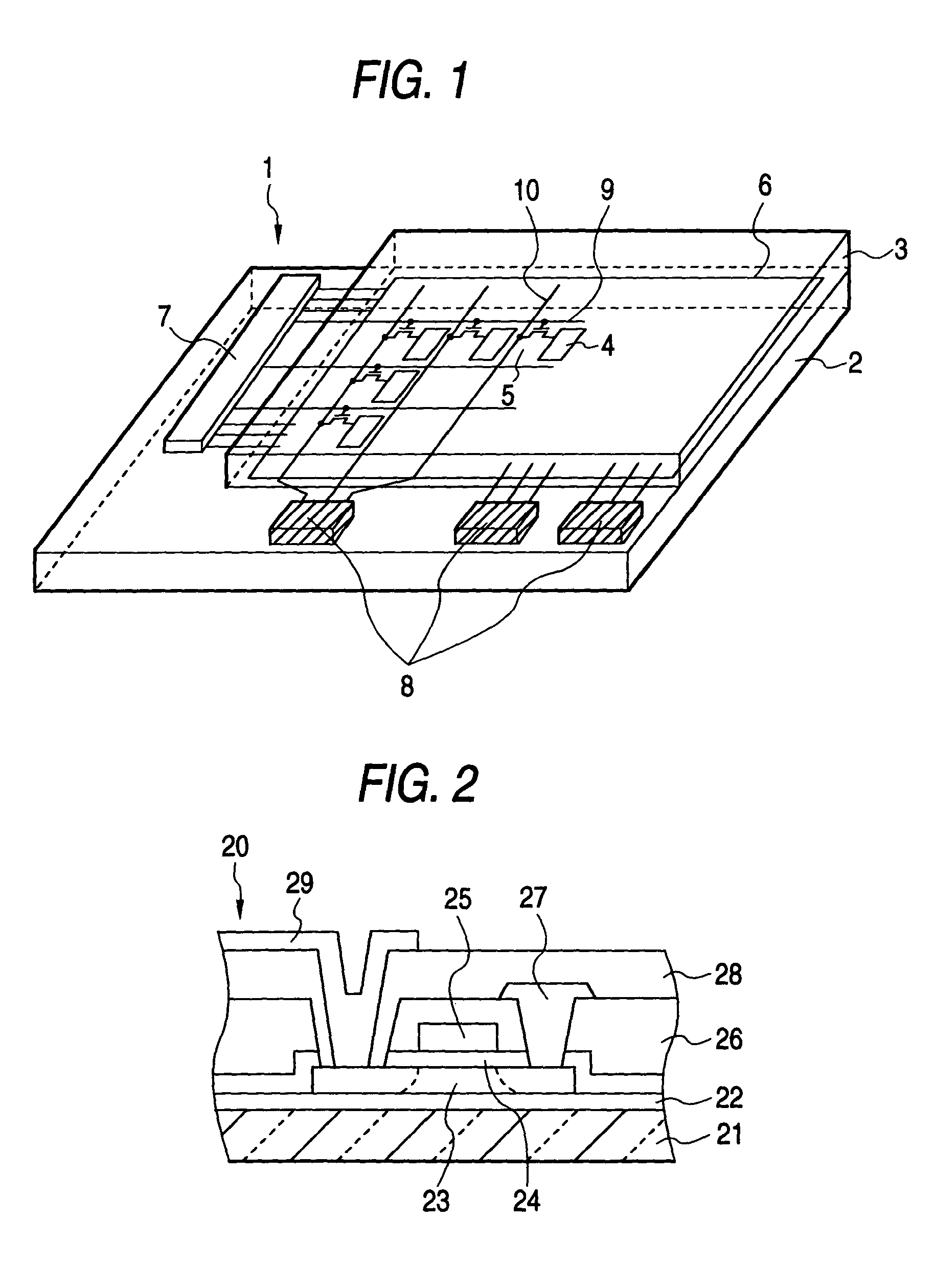
[0028]FIG. 1 is a perspective view showing a liquid crystal display (LCD) 1. The LCD 1 forms an display area by the liquid crystal sealed between a first body substrate 2 and a second body substrate 3 which are made of glass. On the first body substrate 2 in the display area, switching elements 5, which are formed of a plurality of pixel electrodes 4 and thin film transistors (TFT), are arranged in a matrix. Below the second body substrate on the entire surface of the display area, a common electrode 6 is provided. The LCD 1 is a display device in which a voltage is applied between the pixel electrodes 4 and the common electrode 6 to drive the liquid crystal for display. On the periphery of the display area, a single gate line driving IC 7 and a plurality of signal line driving ICs 8 are provided. A plurality of gate lines 9 for respective rows of the pixels are extended from the gate line driving IC 7. The gate line driving IC 7 sequentially selects the gate lines 9 to apply gate s...


PUM


Abstract

Disclosed is an IC chip using a glass substrate capable of being manufactured at a lower cost than the IC chip using from a semiconductor wafer. Further, where the body substrate of a display device is made of glass, the IC chip and the body substrate can have equal coefficients of thermal expansion, thus preventing the IC chips from peeling off and reducing the failure rate. Furthermore, the gate line driving IC applied to a display device can be arranged as an IC chip having a length approximately equal to the display area, therefore, mounting a plurality of IC chips as the gate driving IC is not required, thereby reducing the production cost. Still further, all gate lines can be extended in parallel from the IC chip so that no difference in the delay occurs among the gate lines and the size of frame of display device can reduced.

Description

BACKGROUND OF THE INVENTION[0001]This invention relates to an integrated circuit (IC) chip, and more particularly to an IC chip to be mounted on a glass substrate of a device such as a liquid crystal display (LCD), electroluminescent (EL) display, etc.[0002]In recent years, IC chips are incorporated in not only an information processing device such as a computer, but also various machines such as a television, a household electric appliance, a motor car, etc.[0003]FIG. 6 is a perspective view showing a liquid crystal display (LCD) 100. The LCD 100 forms an display area of the liquid crystal sealed between a first body substrate 2 and a second body substrate 3 which are made of glass. On the first body substrate 2 in the display area, switching elements 5, which are formed of a plurality of pixel electrodes 4 and thin film transistors (TFT), are arranged in a matrix. A common electrode 6 is provided below the second body substrate of the entire surface of the display area. The LCD 10...

Claims


Application Information

Patent Timeline
IPC IPC(8): G02F1/1345G02F1/1333G02F1/1343G02F1/13G02F1/133G02F1/1362G02F1/1368G09F9/00H01L29/786
CPCG02F1/13454G02F1/13452G02F2203/01G02F1/133
Inventor YAMAMURA, KUNIYOKOYAMA, RYOICHIMIYAJIMA, YASUSHIHIROSAWA, KOJI
Owner SANYO ELECTRIC CO LTD
Why Eureka
Try Eureka