Semiconductor memory device including storage nodes and resistors and method of manfacturing the same

a memory device and semiconductor technology, applied in semiconductor devices, capacitors, electrical equipment, etc., can solve the problems of high probability of causing a failure of ocs-type capacitors, large increase in the probability of two-bit failure, and difficulty in forming storage nodes and/or upper electrodes of capacitors with polysilicon as in a conventional technique, so as to achieve sufficient cell capacitance and less susceptible to two-bit failure

Active Publication Date: 2006-09-21
SAMSUNG ELECTRONICS CO LTD
View PDF9 Cites 17 Cited by
  • Summary
  • Abstract
  • Description
  • Claims
  • Application Information

AI Technical Summary

Benefits of technology

[0018] Embodiments of the invention provide a semiconductor memory device including storage nodes and resistors, wherein the semiconductor memory device has a sufficient cell capacitance, is less susceptible to two-bit failure due to leaning or collapsing of the storage nodes, and does not require an additional process for forming resistors on a core / perimeter area.

Problems solved by technology

However, the OCS-type capacitor has a high probability of causing a failure such as a two-bit failure, in which the storage nodes lean to one side or collapse as a result of the design rule reduction.
Furthermore, the probability of a two-bit failure greatly increase if the design rule is reduced below 0.1 μm.
However, when a dielectric film is formed with high-dielectric materials, it is difficult to form storage nodes and / or upper electrodes of a capacitor with polysilicon as in a conventional technique.
Such reaction of a dielectric film and polysilicon may deteriorate the electrical properties of the cell capacitor.
However, if the capacitor electrodes are formed with metal materials, the resistors cannot be formed together when the capacitors are formed.
This is because resistors formed with metal materials have a resistance lower than polysilicon and accordingly a desired voltage cannot be obtained.

Method used


Image

  • Semiconductor memory device including storage nodes and resistors and method of manfacturing the same
  • Semiconductor memory device including storage nodes and resistors and method of manfacturing the same
  • Semiconductor memory device including storage nodes and resistors and method of manfacturing the same

Examples


Embodiment Construction

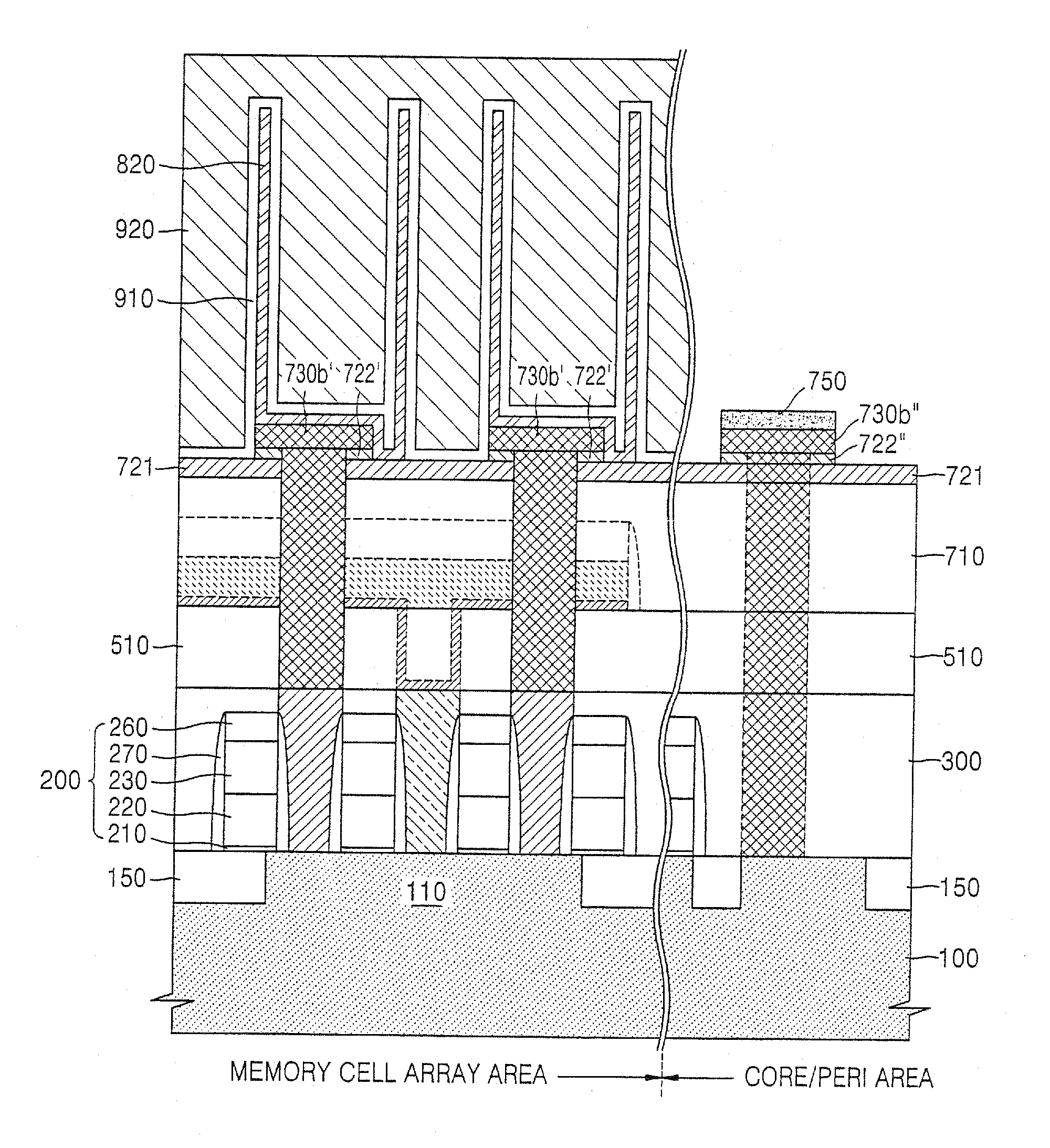
[0023] Hereinafter, several embodiments of the invention will be described in detail with reference to the appended drawings. In the drawings, the thickness of layers may be exaggerated for clarity, and the same reference numerals are used to denote the same elements throughout the drawings.

[0024]FIGS. 2 through 9 are diagram illustrating a semiconductor memory device including storage nodes and resistors and a method of manufacturing the same, according to some embodiments of the invention.

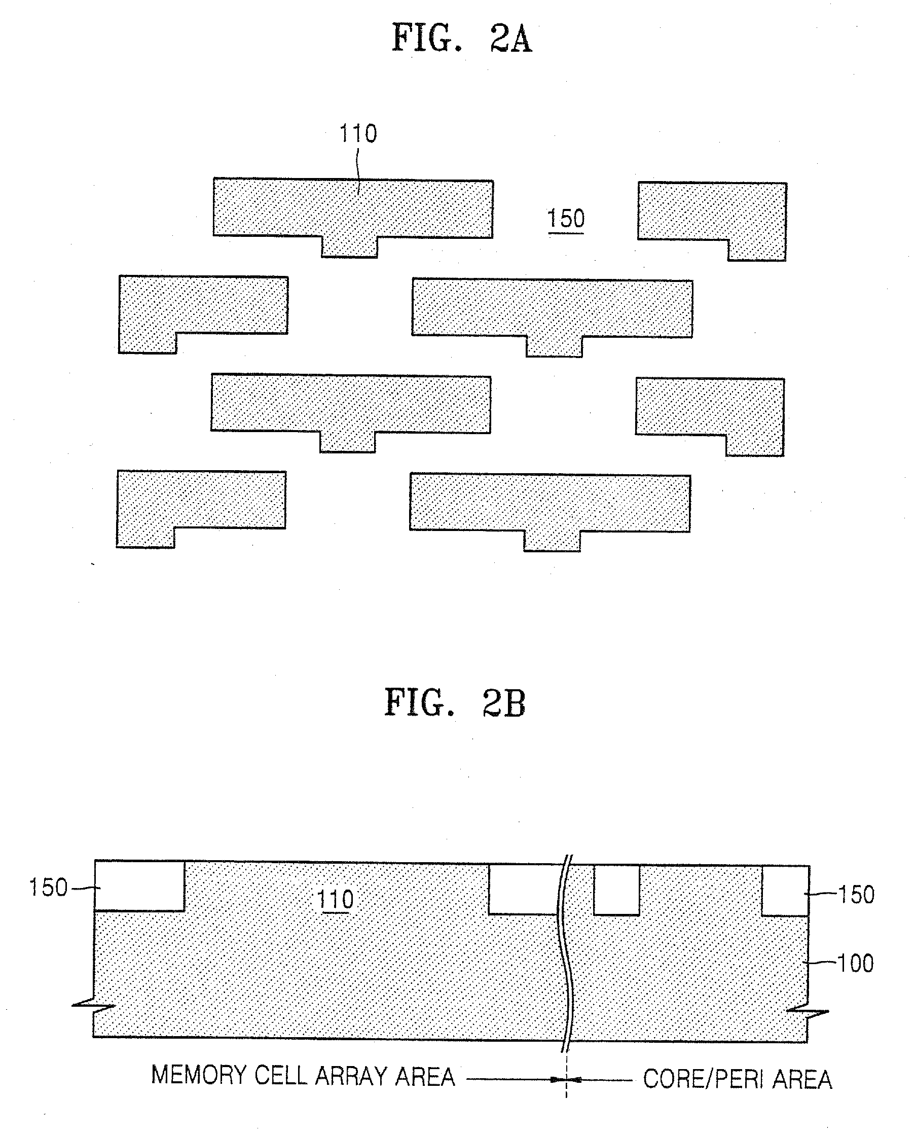
[0025]FIG. 2A is a plan diagram illustrating active areas 110 defined on a memory cell array area of a semiconductor substrate in accordance with some embodiments of the invention. FIG. 2B is a cross-sectional diagram illustrating the memory cell array area of FIG. 2A and an adjacent core / perimeter area.

[0026] Referring to FIGS. 2A and 2B, an active area 110 and an isolation area 150 are defined on a semiconductor substrate 100 including memory cell array areas and core / perimeter areas. A devi...


PUM


Abstract

A semiconductor memory device according to embodiments of the invention includes storage nodes and resistors. A method of manufacturing the semiconductor memory device according to some embodiments of the invention includes forming an interlayer insulation layer on a semiconductor substrate including a memory cell array area and a core / perimeter area; forming a first etch stop layer thereon; forming a plurality of contact plugs arranged linearly in at least one direction on the memory cell array area; forming a first conductive layer on the resultant structure; forming a second etch stop layer thereon; etching the second etch stop layer and the first conductive layer and forming landing pads and resistors arranged non-linearly in at least one direction; and forming storage nodes on the entire outer lateral surfaces of which are exposed, on the landing pads.

Description

CROSS REFERENCE TO RELATED APPLICATIONS [0001] This application is a Divisional of U.S. patent application Ser. No. 10 / 843,837, filed May 11, 2004, now pending, which is claims priority from Korean Patent Application No. 2003-30904, filed on May 15, 2003, which is incorporated by reference in its entirety.BACKGROUND OF THE INVENTION [0002] 1. Field of the Invention [0003] This disclosure relates to a semiconductor device and a method of manufacturing the same, and more particularly, to a semiconductor memory device including storage nodes and resistors and a method of manufacturing the same. [0004] 2. Description of the Related Art [0005] Along with the development of techniques to manufacture semiconductor devices, transistors have become smaller in size and the integration of semiconductor devices has advanced at a rapid pace. In particular, the integration of Dynamic Random Access Memory device (DRAM) has improved rapidly with the development of processing techniques and recently...

Claims


Application Information

Patent Timeline
Patent Type & Authority Applications(United States)
IPC IPC(8): H01L21/8244H01L21/8234H01L21/02H01L21/8242H01L27/02H01L27/108H01L29/76
CPCH01L27/0207H01L27/10855H01L27/10891H01L27/10897H01L28/91H10B12/488H10B12/50H10B12/0335H10B12/00
Inventor CHO, CHANG-HYUNCHUNG, TAE-YOUNGAHN, YONG-SEOK
Owner SAMSUNG ELECTRONICS CO LTD
Why Eureka
Try Eureka