Solder interconnection array with optimal mechanical integrity

a technology of interconnection array and solder ball, which is applied in the direction of soldering apparatus, sustainable manufacturing/processing, and final product manufacturing, etc., can solve the problems of reducing the reliability of thermo-mechanical fatigue (tmf), affecting the integrity of the interconnection, and affecting the interconnection structure. , to achieve the effect of facilitating the joining of the substra

Inactive Publication Date: 2006-03-23
GLOBALFOUNDRIES INC
View PDF22 Cites 18 Cited by
  • Summary
  • Abstract
  • Description
  • Claims
  • Application Information

AI Technical Summary

Benefits of technology

[0016] Bearing in mind the problems and deficiencies of the prior art, it is therefore an object of the present invention to provide methods and apparatus that facilitate joining of a substrate to a board resulting in an electronic module less prone to mechanical and electrical failure, due to both externally applied pressures and thermal cycling expansions during normal working conditions.
[0017] It is another object of the present invention to provide methods and apparatus for enhancing fatigue life properties and preventing short circuits between adjacent solder joints within a solder interconnection grid array residing between a substrate and a circuit board.
[0018] Another object of the invention is to provide methods and apparatus that impose minimal bending stresses on a circuit board, and thereby substantially avoid solder creep flattening to maintain the ball or column shape of a solder interconnection grid array residing between a substrate and the board.

Problems solved by technology

During thermal cycling these CTE mismatch differences can lead to fatigue damage of the solder ball interconnections.
A creep load acting in concert with thermal cycling causes creep or flattening of such solder interconnections, which can result in drastic loss of Thermo-Mechanical Fatigue (TMF) reliability, causing early opens and near-opens in the interconnect structure.
Whereas a full open is a fail, even a near open can have disastrous consequences on electrical performance because of a spike in circuit resistance.
Thus, the accumulation of plastic strains from repeated thermal cycling undesirably deteriorates the long-term reliability of solder joint interconnections, and ultimately leads to fatigue failure of these interconnections residing between the ceramic substrate and the board.
Further adding to fatigue failure of these solder ball interconnections are the pressures applied during the process of attaching a heat sink 5 to the electronic module.
Solder joint creep flattening undesirably deteriorates the long-term reliability of the solder joints and reduces the fatigue lifetime from thermal expansion mismatch among the various components.
In extreme cases, creep flattening of the outer solder interconnections can even result in shorting of adjacent interconnections in the array, which represents catastrophic failure of the electronic module itself.
As solder interconnection array sizes increase, the actual fatigue life (time until failure) of such interconnection array decreases.
However, this approach is not optimal in achieving a useful product life as the second solder interconnection grid array 70 is now susceptible to the deleterious effects of peripheral solder joint 72 solder creep flattening due to the pressures applied during the process of attaching the heat sink 5 to chip 10, as well from any clamping pressure maintained for the life of the assembly.
Further, the addition of an interposer undesirably adds another level of hierarchy to the continually decreasing sized modern electronic component modules.
However, these conventional approaches do not account for or mitigate fatigue stresses on the dual melt solder joints as a result of reducing the effective height of the joint.
These approaches are also not useful for dual melt solder interconnections due to the eutectic solder of the dual melt solder which undergoes a 3-4% volumetric expansion upon liquation during card attach, whereby the resultant hydrostatic stresses will easily rupture the cured epoxy encapsulant.
Further, these conventional approaches are not useful for single melt solders because the encapsulant will have no adhesion to the single melt solder during reflow operations.
Further, while underfill processes enhance solder interconnection reliability, they are quite sensitive to the material flow properties of the liquid resin, and their success is highly dependent upon module geometry.
Modules built with larger chips, e.g., greater than 20 mm on a side, and very densely populated arrays, are more difficult to underfill than those built with smaller chips.
Also, this type of processing is not easily extended to large solder interconnection grid arrays, e.g., those having solder joint gap heights (i.e., the height of the gap between the substrate to the board) of about 300 microns to about 900 microns, as is the case in solder arrays residing between a substrate and a circuit board.
Problems with adhesion, gap (height) filling, voiding and flow control, particularly in solder interconnection grid arrays having gap heights ranging from about 300-900 microns, are difficult to control.
Any flexing or bending of the circuit board ultimately leads to solder creep flattening within the solder interconnection grid array joining the substrate to the board.
However, the use of backing plates undesirably increases costs of the electronic module, adds additional thickness to the assembly, increases processing steps and prevents the use of capacitors or modules at the back of the board.

Method used


Image

  • Solder interconnection array with optimal mechanical integrity
  • Solder interconnection array with optimal mechanical integrity
  • Solder interconnection array with optimal mechanical integrity

Examples


Embodiment Construction

)

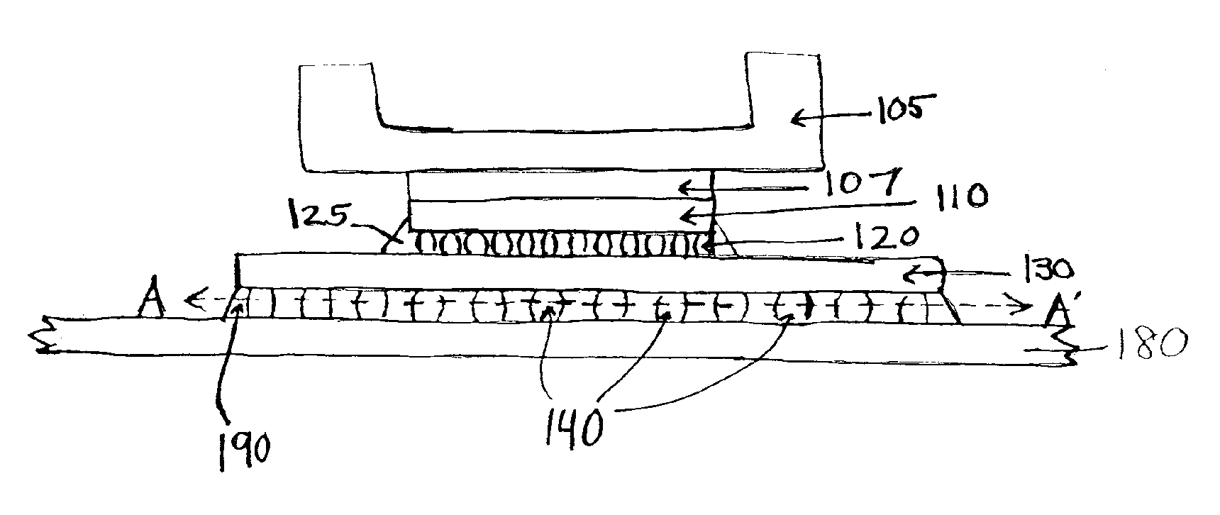
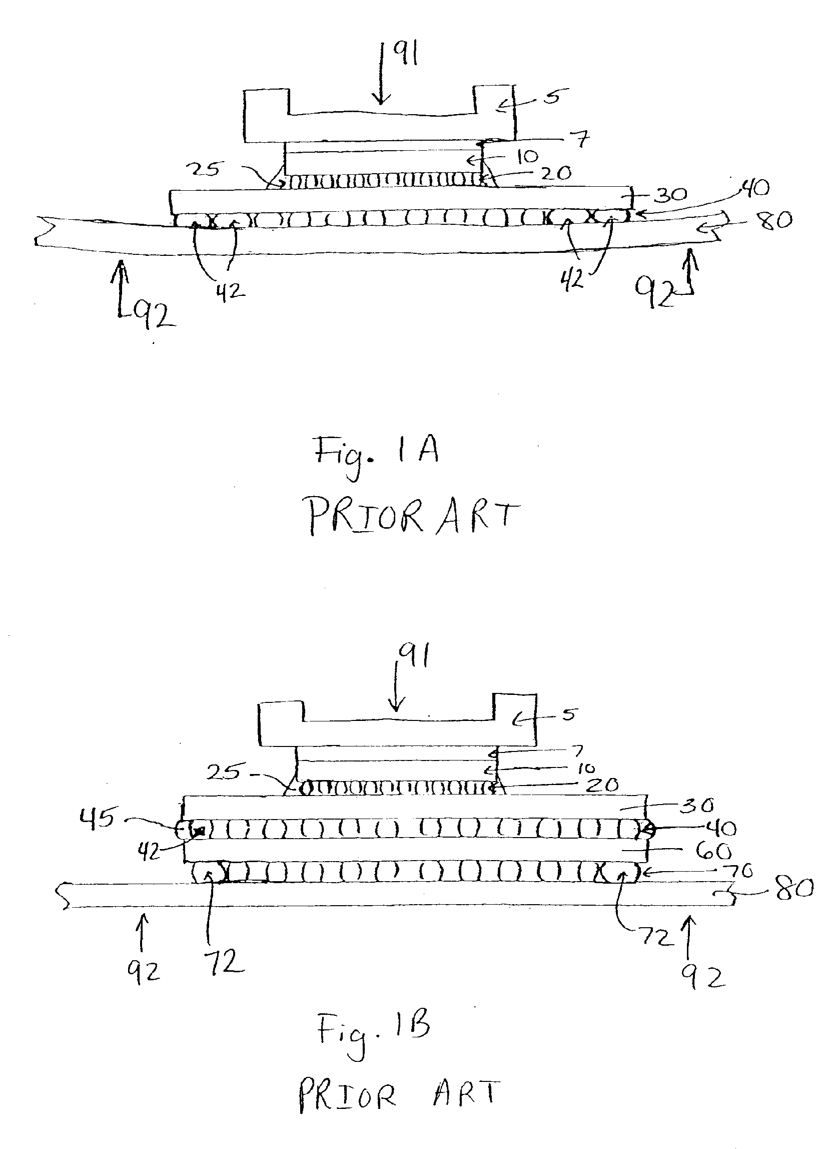
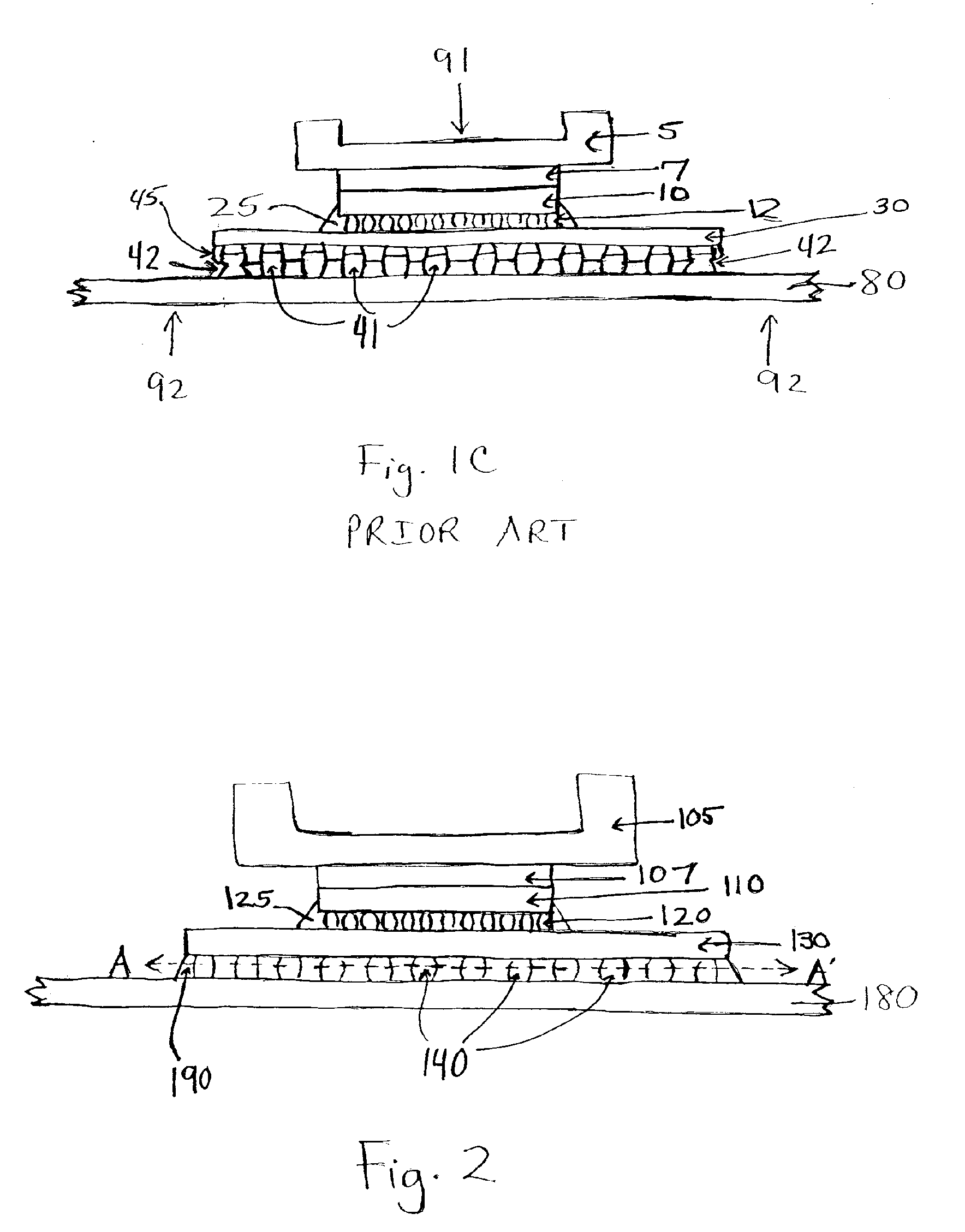
[0050] In describing the preferred embodiment of the present invention, reference will be made herein to FIGS. 2-15 of the drawings in which like numerals refer to like features of the invention.

[0051] Referring to FIG. 2, an electronic module is shown that includes a chip 110 mounted on a substrate or chip carrier 130 by known mounting means, such as a solder interconnection grid array 120, e.g., C4 connections 120. A chip underfill material 125 encapsulates at least a portion, and preferably all, of the C4 connections 120 to improve the solder ball fatigue reliability and to provide an effective barrier against environmental and process exposures. This chip underfill material 125 may include any known underfill material for encapsulating solder interconnections between a chip and a substrate. The substrate 130 may comprise a ceramic substrate, an organic substrate, a silicon substrate or a variety of other known substrate materials.

[0052] Once the chip is joined to the chip car...


PUM

PropertyMeasurementUnit
gap heightsaaaaaaaaaa
viscosityaaaaaaaaaa
densityaaaaaaaaaa

Abstract

A method for assembling, and the resultant electronic module, includes attaching a chip to a substrate using a first solder interconnection array, and attaching a board to the substrate using a second solder interconnection array, which may be a single-melt or a dual-melt solder array. The second solder interconnection array resides entirely within a space defined between the board and substrate. A creep resistant structure is provided within this space for maintaining the defined space and optimizing integrity of the second solder interconnection array. The creep resistant structure may include an underfill material, balls, brackets, frames, collars or combinations thereof. Wherein the creep resistant structure is an underfill material, it is crucial that the substrate be attached to the board before either entirely encapsulating the second interconnection array with underfill material, or partially encapsulating the second solder interconnection array at discrete locations with underfill material.

Description

BACKGROUND OF THE INVENTION [0001] 1. Field of the Invention [0002] The present invention relates generally to the packaging and mounting of semiconductor devices in electronic circuits, and in particular, to a method and apparatus for optimizing the integrity of a solder interconnection joining a substrate to an organic circuit board. [0003] 2. Description of Related Art [0004] Modern electronic modules include microchips and other circuit components mounted on chip carrier substrates, which in turn, are mounted to printed circuit boards. In the electronics area there is a myriad of electronic components that require connection to other electronic components, or to other levels of packaging. Examples include mounting of integrated circuit chips to a metallized substrate, multilayer ceramic substrate (MLC), laminate organic substrate, glass ceramic substrate, card (direct-chip-attach), and any substrate made of composite materials meeting thermal and mechanical properties. The use o...

Claims


Application Information

Patent Timeline
Patent Type & Authority Applications(United States)
IPC IPC(8): B23K31/02
CPCB23K3/0638Y10T29/49144H05K3/301H05K3/303H05K3/305H05K2201/0209H05K2201/09909H05K2201/10234H05K2201/10734H05K2201/10977H05K2201/2018H05K2201/2036H01L2224/16225H01L2224/32225H01L2224/73204H01L2224/73253H01L2924/15311B23K2201/40H01L2924/01322H01L2924/00012H01L2924/00B23K2101/40H01L2924/00011H01L2924/00014Y02P70/50H01L2224/0401
Inventor DAVES, GLENN G.EDWARDS, DAVID L.FAROOQ, MUKTA G.POMPEO, FRANK L.
Owner GLOBALFOUNDRIES INC
Why Eureka
Try Eureka