Double-sampled, time-interleaved analog to digital converter

a time-interleaved analog and digital converter technology, applied in the field of electronic devices, can solve the problems of reducing the signal to noise (snr) of the combined sub-sample signal, affecting the performance of the operation amplifier, and affecting the quality of the output signal,

Active Publication Date: 2006-07-11
AVAGO TECH INT SALES PTE LTD
View PDF12 Cites 37 Cited by
  • Summary
  • Abstract
  • Description
  • Claims
  • Application Information

AI Technical Summary

Benefits of technology

[0010]The invention includes an apparatus and method for high-speed analog to digital sample conversion.

Problems solved by technology

The time interleaved ADC architecture of FIG. 1, however, has several limitations.
For example, this time interleaved ADC architecture can suffer from gain errors, offset errors and phase timing errors, resulting in degradation of the signal to noise (SNR) of the combined sub-sample signals.
Operational amplifiers dissipate a relatively large amount of power.
Therefore, time interleaved ADC systems can dissipate more power than desired.

Method used


Image

  • Double-sampled, time-interleaved analog to digital converter
  • Double-sampled, time-interleaved analog to digital converter
  • Double-sampled, time-interleaved analog to digital converter

Examples


Embodiment Construction

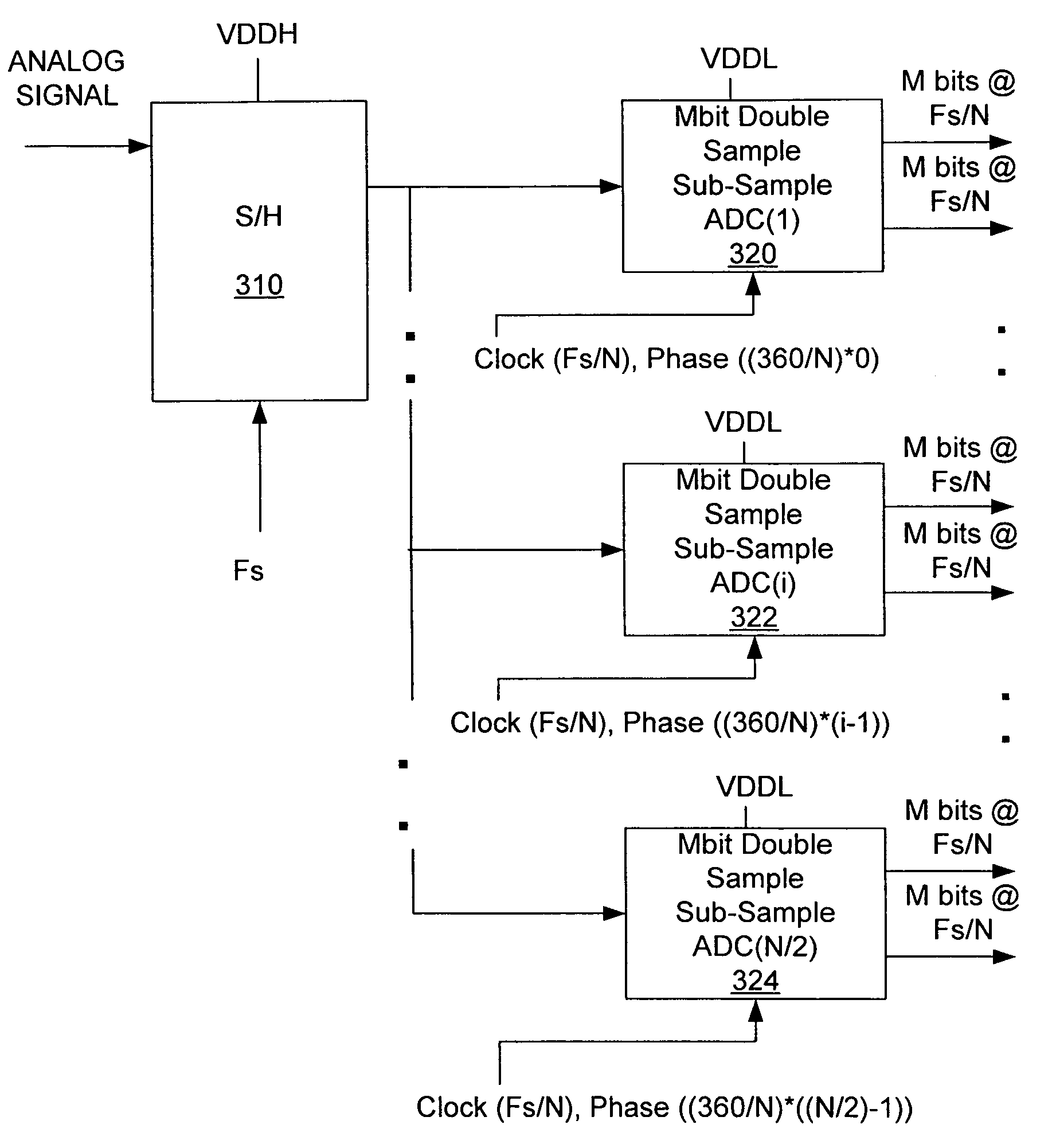
[0026]As shown in the drawings for purposes of illustration, the invention is embodied in an apparatus and method for high-speed analog to digital sample conversion.

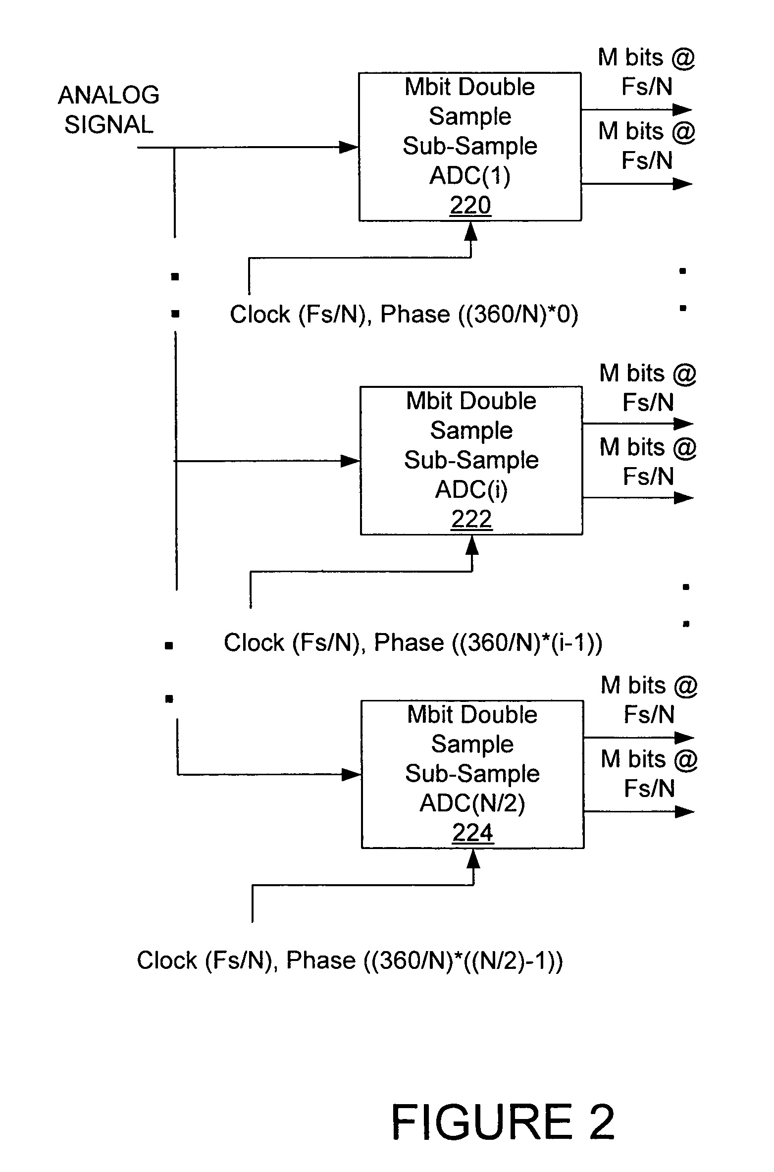
[0027]FIG. 2 shows time interleaved, double sampled ADC system. The time-interleaved ADC system includes N / 2 sub-ADCs 220, 222, 224. Each sub-ADC 220, 222, 224 receives an analog signal (ANALOG SIGNAL) and a clock signal. Each sub-ADC 220, 222, 224 generates two digital samples at a rate of Fs / N, the two digital samples are generated with approximately 180 degree phase relationship relative to a frequency of Fs / N. The time-interleaved ADC system generates output samples at a rate of Fs, by combining the digital samples generated by the sub-ADC 220, 222, 224.

[0028]As shown in FIG. 2, each of the sub-ADCs 220, 222, 224 receive a clock signal. The clock signals shown in FIG. 2 are delayed in phase by (360 / N)*(i−1) where i varies from 1 to N / 2. As stated above, each sub-ADCs 220, 222, 224 generates two samples at a rate of F...


PUM


Abstract

An apparatus and method for high-speed analog to digital conversion are disclosed. An ADC system includes a plurality of N/2 sub-ADCs, each sub-ADC receiving an analog signal and a clock signal and generating two digital samples at a rate of Fs/N. The two digital samples are generated with approximately 180 degree phase relationship relative to a frequency of Fs/N. The plurality of N/2 sub-ADCs of the time-interleaved ADC system, generate combined output samples at a rate of Fs. An ADC method includes a plurality of N/2 sub-ADCs receiving the analog signal, clocking each sub-ADC at a rate of FS/N. Each sub-ADC generates two digital samples at a rate of FS/(2N), the two digital samples being generated with approximately 180 degree phase relationship relative to a frequency of Fs/N. Outputs of the sub-ADCs are combined to generate digital samples at a rate of Fs.

Description

FIELD OF THE INVENTION[0001]The invention relates generally to electronics. More particularly, the invention relates to a double sampled, time interleaved analog to digital converter.BACKGROUND OF THE INVENTION[0002]High-speed networks are continually evolving. The evolution includes a continuing advancement in the operational speed of the networks. The network implementation of choice that has emerged is Ethernet networks physically connected over twisted pair wiring. One of the most prevalent high speed LANs (local area network) for providing connectivity between personal computers, workstations and servers is Ethernet in its 10BASE-T form.[0003]High-speed LAN technologies include 100BASE-T (Fast Ethernet) and 1000BASE-T (Gigabit Ethernet). Fast Ethernet technology has provided a smooth evolution from the 10 megabits per second (Mbps) performance of 10BASE-T to the 100 Mbps performance of 100BASE-T. Gigabit Ethernet provides 1 Gigabit per second (Gbps) data rate with essentially t...

Claims


Application Information

Patent Timeline
Patent Type & Authority Patents(United States)
IPC IPC(8): H03M1/12
CPCH03M1/1215
Inventor GUPTA, SANDEEP KUMAR
Owner AVAGO TECH INT SALES PTE LTD
Why Eureka
Try Eureka