

Non-volatile memory device with protruding charge storage layer and method of fabricating the same
- Summary
- Abstract
- Description
- Claims
- Application Information
AI Technical Summary
Benefits of technology
Problems solved by technology
Method used
Image

Examples
first embodiment
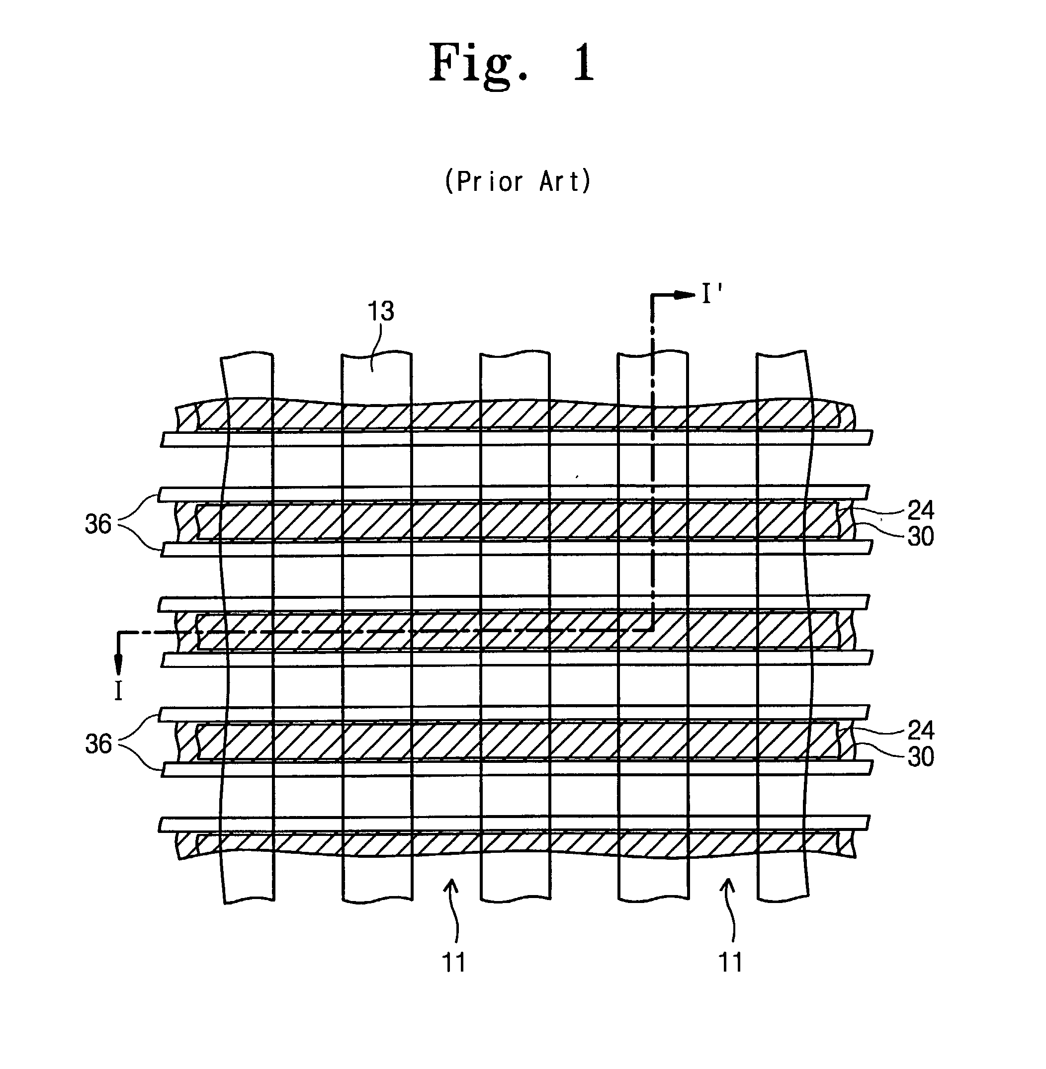
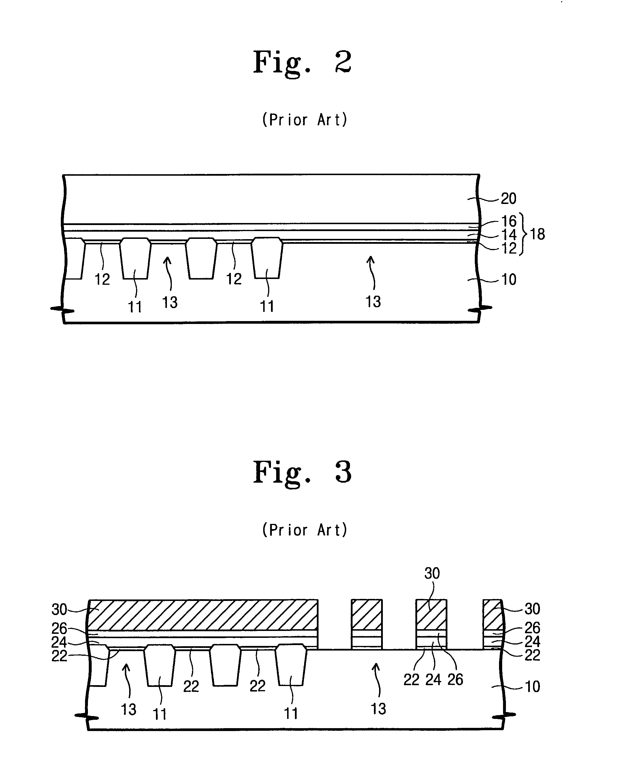
[0034]FIG. 8 through FIG. 11 are cross-sectional flow diagrams showing the steps of fabricating a non-volatile memory device according to the present invention, taken along a line II–II of FIG. 6.
[0035]Referring now to FIG. 8, a device isolation layer 101 is formed in a semiconductor substrate 100 to define a first active region 103 and a second active region 203 in a cell array region “a” and a peripheral circuit region “b”, respectively. A stacking insulating layer 108 and a gate conductive layer 120 are sequentially formed in a cell array region “a” of a semiconductor substrate 100 where the device isolation layer 101 is formed. At the same time, a gate insulating layer 108 and a gate conductive layer 120 are sequentially formed in a peripheral region “b” of the semiconductor substrate where the device isolation layer 101 is formed. Preferably, the stack insulating layer 108 is formed by sequentially stacking first, second, and third insulating layers 102, 104, and 106. Preferabl...
second embodiment
[0043]FIG. 12 through FIG. 14 are cross-sectional flow diagrams for explaining the steps of fabricating a non-volatile memory device according to the present invention.
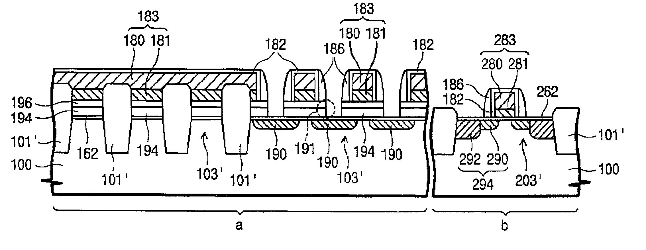
[0044]Referring now to FIG. 12, steps until formation of a gate conductive layer 120 (see FIG. 8) in the second embodiment are identical to those in the first embodiment, as described in FIG. 8. The gate conductive layer 120 and the third insulating layer 106 (see FIG. 8) are sequentially patterned to form a wordline 140 and a third insulating layer pattern 156a on the second insulating layer 104 in the cell array region “a” and to form a gate electrode 240 in the peripheral circuit region “b”. The third insulating layer pattern 156 corresponds to a blocking insulating layer. Furthermore, a thermal oxidation process is carried out for the semiconductor substrate to form a gate capping oxide layer 142′ on a sidewall and a top surface of the wordline 140 and the gate electrode 240.
[0045]Referring now to FIG. 13, in the ...
third embodiment
[0056]FIG. 17 through FIG. 19 are cross-sectional flow diagrams for explaining the steps of fabricating the non-volatile memory device according to the present invention, taken along a line III–III′ of FIG. 15.
[0057]Referring now to FIG. 17, a stack insulating layer 168 is formed on a semiconductor substrate 100. After the stack insulating layer 168 formed in a peripheral circuit region “b” is removed and a gate insulating layer 262 is formed, a lower gate conductive layer 169 and a hard mask layer are formed on an entire surface of the substrate 100. The hard mask layer, the lower gate conductive layer 169, the stack insulating layer 168, and the substrate 100 in a cell array region “a” and the hard mask layer, the lower gate electrode 169, and the substrate 100 are sequentially patterned to form a trench in a predetermined area of the substrate 100. Preferably, the first insulating layer 162 is formed to a thickness of 15 Å–35 Å in order to make a tunneling of charges even in low ...
PUM
 Abstract
Description
Claims
Application Information