
Power semiconductor device having a voltage sustaining region that includes terraced trench with continuous doped columns formed in an epitaxial layer

a technology of semiconductor devices and electrodes, applied in the field of semiconductor devices, can solve the problems of difficult to avoid non-uniformities in the dopant gradient of columns, rapid increase in resistance of devices, and difficult to resist rapid increase in resistan

Inactive Publication Date: 2006-08-01
GEN SEMICON
View PDF49 Cites 12 Cited by
  • Summary
  • Abstract
  • Description
  • Claims
  • Application Information

AI Technical Summary

Problems solved by technology

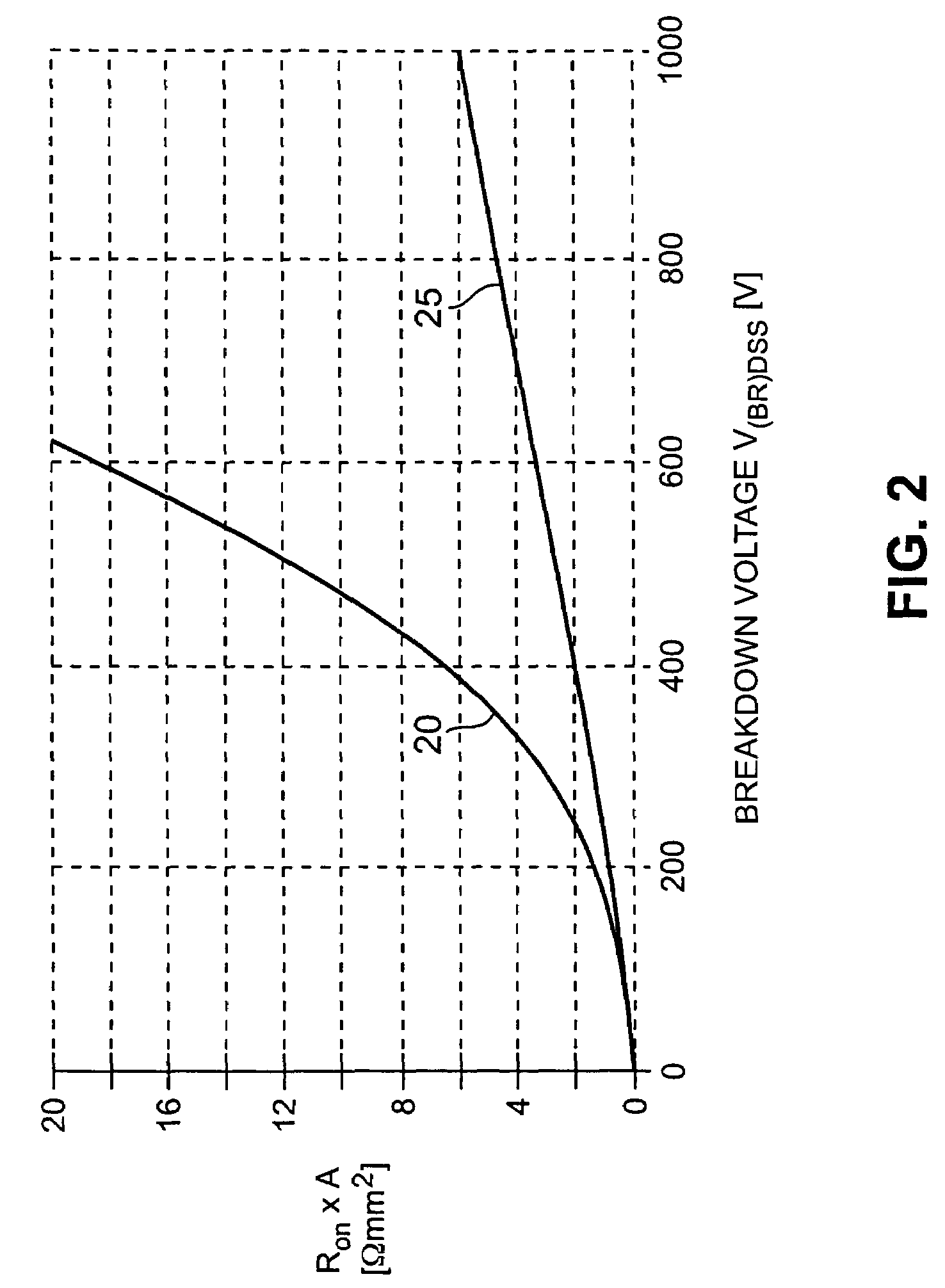
Unfortunately, as curve 20 shows, the on-resistance of the device increases rapidly as its breakdown voltage increases.
This rapid increase in resistance presents a problem when the MOSFET is to be operated at higher voltages, particularly at voltages greater than a few hundred volts.
Unfortunately, nonuniformities in the dopant gradient of the columns can be difficult to avoid as a result of limitations in the control of process parameters during their fabrication.
Unfortunately, epitaxial deposition steps are expensive to perform and thus this structure is expensive to manufacture.
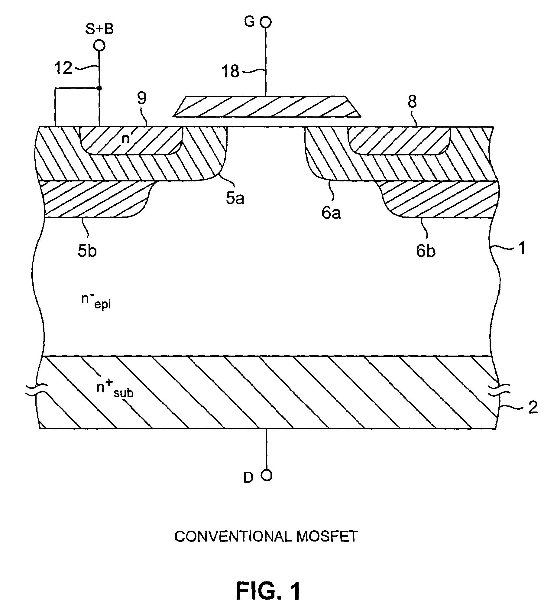
However, the on-resistance of a device that uses the floating island technique is not as low as an identical device that uses continuous columns.

Method used


Image

  • Power semiconductor device having a voltage sustaining region that includes terraced trench with continuous doped columns formed in an epitaxial layer
  • Power semiconductor device having a voltage sustaining region that includes terraced trench with continuous doped columns formed in an epitaxial layer
  • Power semiconductor device having a voltage sustaining region that includes terraced trench with continuous doped columns formed in an epitaxial layer

Examples


Embodiment Construction

[0022]In accordance with the present invention, a method of forming the p-type columns in the voltage sustaining layer of a semiconductor power device may be generally described as follows. First, a terraced trench is formed in the epitaxial layer that is to form the voltage sustaining region of the device. The terraced trench is formed from two or more co-axially located trenches that are etched at different depths in the epitaxial layer. The diameter of each individual trench is greater than the diameter of the trenches located at greater depths in the epitaxial layer. Adjacent trenches meet in horizontal planes to define annular ledges, which arise from the differential in the diameter of the adjacent trenches. P-type dopant material is implanted into both the annular ledges and the bottom of the deepest trench in a single implantation step. The implanted material is diffused into the portion of the voltage sustaining region located immediately adjacent to and below the ledges an...


PUM


Abstract

A method is provided for forming a power semiconductor device. The method begins by providing a substrate of a first conductivity type and forming a voltage sustaining region on the substrate. The voltage sustaining region is formed in the following manner. First, an epitaxial layer is deposited on the substrate. The epitaxial layer has a first or a second conductivity type. Next, at least one terraced trench is formed in the epitaxial layer. The terraced trench has a trench bottom and a plurality of portions that differ in width to define at least one annular ledge therebetween. A barrier material is deposited along the walls and bottom of the trench. A dopant of a conductivity type opposite to the conductivity type of the epitaxial layer is implanted through the barrier material lining the annular ledge and at the trench bottom and into adjacent portions of the epitaxial layer to respectively form at least one annular doped region and another doped region. The dopant is diffused in the annular doped region and the another doped region to cause the regions to overlap one another, whereby a continuous doped column is formed in the epitaxial layer. A filler material is deposited in the terraced trench to substantially fill the terraced trench. Finally, at least one region of conductivity type opposite to the conductivity type of the epitaxial layer is formed over the voltage sustaining region to define a junction therebetween.

Description

STATEMENT OF RELATED APPLICATIONS[0001]This application is a divisional application of U.S. patent application Ser. No. 10 / 103,674, filed Mar. 21, 2002 now U.S. Pat. No. 6,686,244, entitled “Power Semiconductor Device Having A Voltage Sustaining Region That Includes Doped Columns Formed With A Single Ion Implantation Step.”[0002]This application is related to U.S. patent application Ser. No. 09 / 970,972 entitled “Method for Fabricating a Power Semiconductor Device Having a Floating Island Voltage Sustaining Layer,” filed in the United States Patent and Trademark Office on Oct. 4, 2001, now U.S. Pat. No. 6,465,304.[0003]This application is related to U.S. patent application Ser. No. 10 / 039,068 entitled “Method For Fabricating A High Voltage Power MOSFET Having A Voltage Sustaining Region That Includes Doped Columns Formed By Rapid Diffusion,” filed in the United States Patent and Trademark Office on Dec. 31, 2001, now U.S. Pat. No. 6,566,201.[0004]This application is related to U.S. p...

Claims


Application Information

Patent Timeline
IPC IPC(8): H01L29/78H01L21/336H01L29/06
CPCH01L29/0634H01L29/7802H01L29/66712H01L29/0649H01L29/1095
Inventor BLANCHARD, RICHARD A.
Owner GEN SEMICON
Learn More