Optical multi/demultiplexing circuit equipped with phase generating device

a phase generation device and multi-multiplexing technology, applied in multiplex communication, optical elements, instruments, etc., can solve the problems of wavelength dependence of path length difference between l and wavelength dependence of conventional optical couplers such as directional couplers and multi-mode interferometers

Inactive Publication Date: 2006-08-01
NIPPON TELEGRAPH & TELEPHONE CORP
View PDF20 Cites 24 Cited by
  • Summary
  • Abstract
  • Description
  • Claims
  • Application Information

AI Technical Summary

Benefits of technology

[0043]Using the optical multi/demultiplexer equipped with phase generating device in accordance with the present invention can implement the uniform period transmission characteristics even on the wavelength axis, thereby being able to provide an optical device applicable to optical communication systems with uniform wavelength period.
[0044]In addition, using the phase ...

Problems solved by technology

The conventional optical coupler such as a directional coupler and multimode interferometer used in ...

Method used


Image

  • Optical multi/demultiplexing circuit equipped with phase generating device
  • Optical multi/demultiplexing circuit equipped with phase generating device
  • Optical multi/demultiplexing circuit equipped with phase generating device

Examples


first embodiment

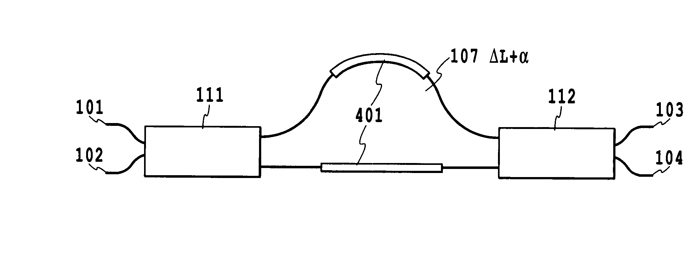
[0138]FIG. 4 shows a first embodiment of the optical multi / demultiplexing circuit in accordance with the present invention. The present embodiment includes two two-input / two-output phase generating optical couplers 111 and 112; an optical delay line section 107 consisting of two optical waveguides between the two phase generating optical couplers 111 and 112; and two input / output optical waveguides 101 and 102, and 103 and 104 connected to the phase generating optical couplers 111 and 112.

[0139]The optical multi / demultiplexing circuit has a function (phase generating function) for correcting the deviation of the wavelength period so that the transmission characteristics have an approximately uniform period on the wavelength axis. The function can be achieved by configuring at least one of the phase generating optical couplers 111 and 112 in such a fashion that the output phase difference of the phase generating optical coupler has a wavelength dependence in the passband of the optic...

second embodiment

[0174]FIG. 14 shows a second embodiment of the optical multi / demultiplexing circuit in accordance with the present invention. The present embodiment includes two phase generating optical couplers 111 and 112 whose output phase differences have a wavelength dependence in the passband; an optical delay line section 107 between the two phase generating optical couplers 111 and 112; and two input / output optical waveguides 101 and 102, and 103 and 104 connected to the phase generating optical couplers 111 and 112, respectively.

[0175]The two phase generating optical couplers 111 and 112 are each configured as shown in FIG. 15. They include four optical couplers 201–204, and three optical delay line sections 205–207 between the adjacent optical couplers 201–204.

[0176]The multi / demultiplexing circuit has the transmission characteristics with approximately uniform period on the wavelength axis. In addition, to achieve such a transmission characteristics, the deviation between the uniform wav...

third embodiment

[0195]FIG. 19 shows a third embodiment of the multi / demultiplexing circuit in accordance with the present invention. The circuit includes three phase generating optical couplers 111, 112 and 113; two optical delay line sections 107 and 108 between the three phase generating optical couplers; two input / output optical waveguides 101 and 102 connected to the phase generating optical coupler 111; and two input / output optical waveguides 103 and 104 connected to the phase generating optical coupler 113.

[0196]The path length difference of the optical delay line section 107 is set at ΔL1′=ΔL1+α1, and that of the optical delay line section 108 is set at ΔL2′=ΔL2+α2, where α1 and α2 are path lengths of the wavelength order as described in the first embodiment.

[0197]In addition, at least one of the three optical multi / demultiplexing devices consists of a phase generating optical coupler, and the phase difference between the outputs varies corresponding to wavelength in the passband of the inte...


PUM


Abstract

An optical multi/demultiplexing circuit includes at least one phase generating optical coupler and an optical delay line coupled to the phase generating optical coupler. The phase generating optical coupler consists of at least one input and at least two outputs. At least one of the phase generating optical coupler has a wavelength dependent or frequency dependent output phase difference in the passband of the circuit so that it can change the transmittance characteristics of the optical multi/demultiplexing circuit.

Description

[0001]This application claims priority from Japanese Patent Application No. 2002-354640 filed Dec. 6, 2002, which is incorporated hereinto by reference.BACKGROUND OF THE INVENTION[0002]1. Field of the Invention[0003]The present invention relates to an optical multi / demultiplexing circuit used in an optical communication field, and particularly to an optical multi / demultiplexing circuit used for wavelength division multiplexing.[0004]2. Description of the Related Art[0005]With the recent development of dense wavelength division multiplexing (DWDM) systems, optical devices with a variety of functions which are essential for the WDM systems have been developed such as wavelength multi / demultiplexers, optical filters and optical switches.[0006]As examples of the optical devices, the following devices are reported: an arrayed waveguide grating and lattice-form filter (see, for example, M. Oguma et al. “Passband-width broadening design for WDM filter with lattice-form interleave filter an...

Claims


Application Information

Patent Timeline
IPC IPC(8): G02B6/26G02B6/12G02B6/122G02B6/34
CPCG02B6/12007G02B6/12016G02B6/12019G02B6/2938G02B6/12023G02B6/29353G02B6/29355G02B6/12021
Inventor MIZUNO, TAKAYUKIKITOH, TSUTOMUOGUMA, MANABUINOUE, YASUYUKI
Owner NIPPON TELEGRAPH & TELEPHONE CORP
Why Eureka
Try Eureka