Die bonding method and apparatus

Active Publication Date: 2006-08-08
SHINKAWA CO LTD
View PDF6 Cites 4 Cited by
  • Summary
  • Abstract
  • Description
  • Claims
  • Application Information

AI Technical Summary

Benefits of technology

[0010]Accordingly, the object of the present invention is to provide a die bonding method and apparatus that

Problems solved by technology

However, there are cases in which the pitch of the chip-mount portions deviates because of the heat that is generated during bonding, etc.
Accordingly, since an inspection process is added following the die bonding process, there are problems in terms of the production time and human labor required.
Furthermore, since there is a time difference between the die bonding process and the inspection process, there is a delay in the detection of abnormalities in cases where such abnormalities occur in the die bonding apparatus, resulting in the generation of a large quantity of defective products.
However, in the above die bonding apparatus, a camera that images the chip-mount portions prior to bonding cannot be installed; and thus, detection of the bonding positions is impossible.
However, in the case of such a joint installation of two cameras, there is a distance between the cameras, and the chip-mount portions imaged by the respective cameras are separated from each other.
Accordingly, the chip-mount portions on which bonding has just been performed cannot be

Method used


Image

  • Die bonding method and apparatus
  • Die bonding method and apparatus
  • Die bonding method and apparatus

Examples


Embodiment Construction

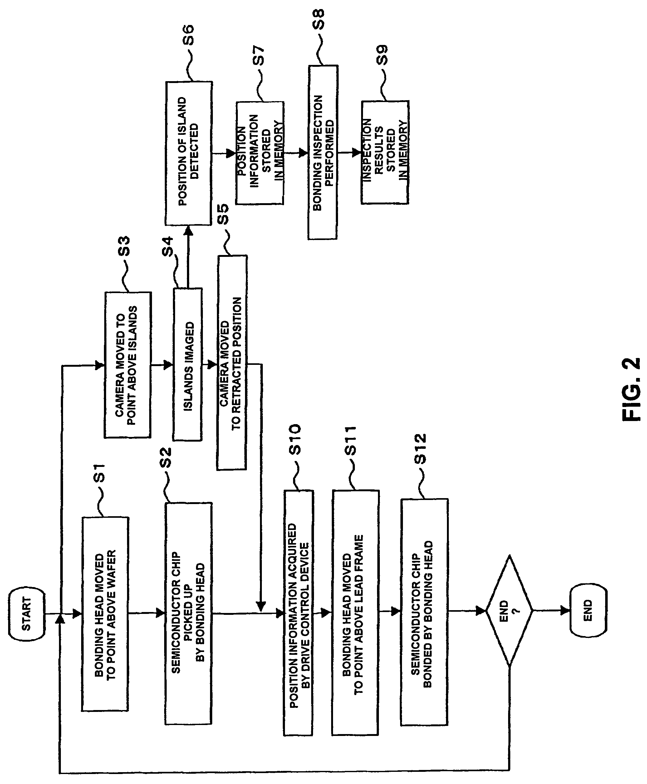
[0025]Embodiments of the present invention will be described below with reference to the accompanying drawings.

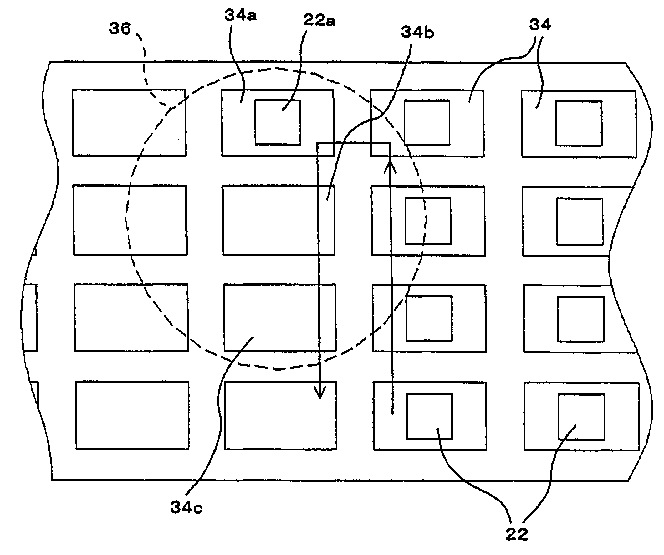
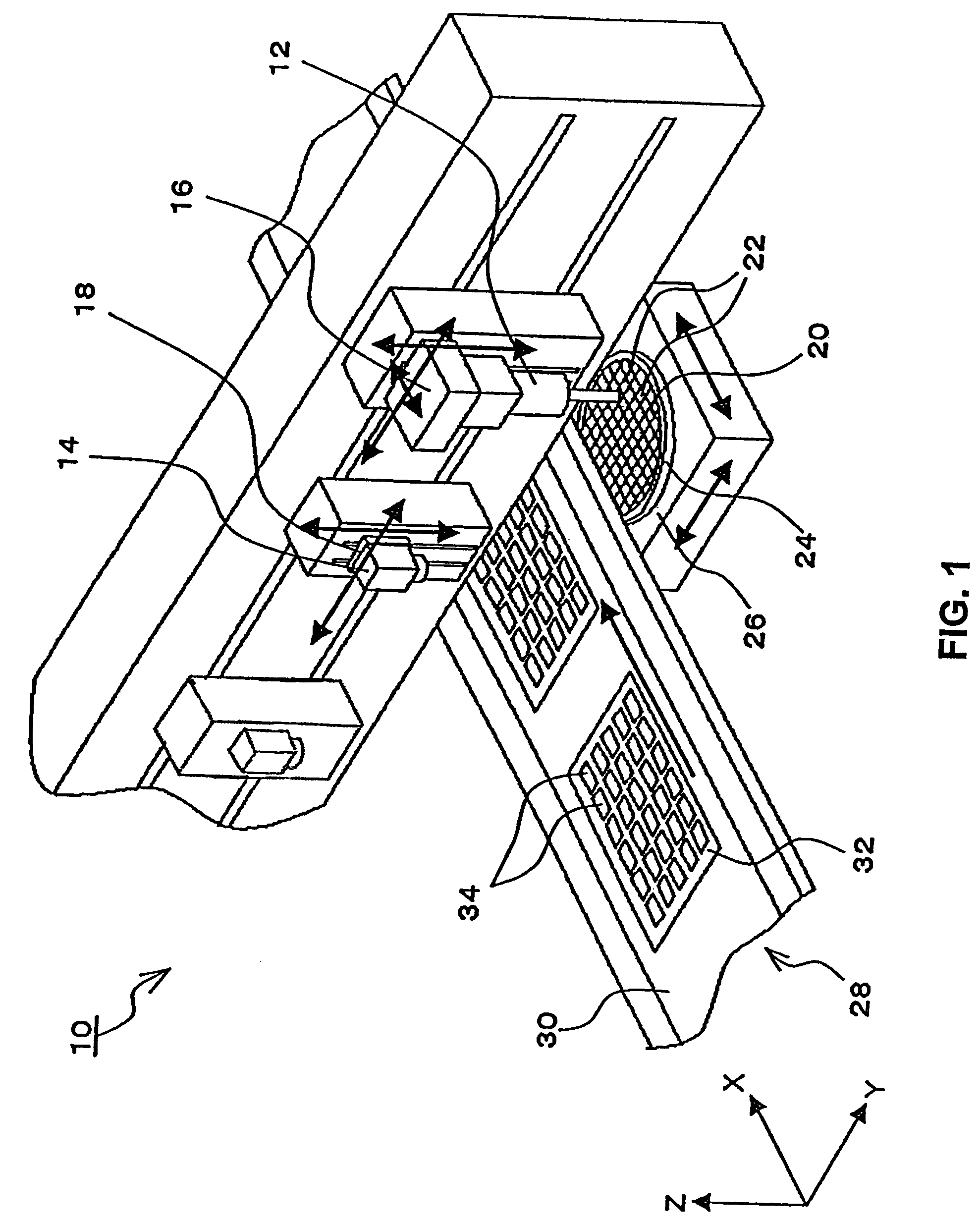
[0026]FIG. 1 shows a die bonding apparatus 10 of an embodiment of the present invention. This apparatus comprises: a bonding head 12 which performs bonding, a CCD (charge-coupled device) camera 14 which is used to image islands 34 that constitute chip-mount portions disposed on a lead frame 32, a conveying apparatus 28 which is used to convey the lead frame 32, and a wafer holder 24 which holds a wafer 20.

[0027]The bonding head 12 has a central axis that is oriented in the vertical direction, and it is held by a head moving table 16. The bonding head 12 can be moved in the Y and Z directions (or horizontally) by driving the head moving table 16, and very slight movement in the X direction is also possible. A suction part which is used for suction chucking and release of semiconductor chips 22 formed in the wafer 20 is disposed on the tip end portion of the bonding head 12.

[...


PUM


Abstract

A die bonding method and apparatus that performs bonding position detection and bonding inspection without lowering the productivity, in which after a bonding head has bonded a semiconductor chip to an island, the bonding head is moved to a wafer to pick up a semiconductor chip and is returned to the island; and during this period, an island used for bonding inspection (that is the island on which bonding has just been performed) and an island used for position detection (that is the island on which bonding is to be done next) are imaged by a camera in the same visual field, and inspection of the bonding conditions of the island used for inspection and detection of the position of the island used for position detection are performed based on the acquired image data.

Description

BACKGROUND OF THE INVENTION[0001]1. Field of the Invention[0002]The present invention relates to a die bonding method and apparatus in which chips are successively bonded to a plurality of chip-mount portions disposed on a substrate.[0003]2. Prior Art[0004]In die bonding processes performed in the manufacture of semiconductors, a die bonding apparatus is used for the successive bonding of semiconductor chips to chip-mount portions such as islands, etc., that are disposed on a substrate. The chip-mount portions are disposed at a uniform pitch on the substrate; and when bonding is performed, the positional control of the driving of the bonding head is performed based on this pitch. However, there are cases in which the pitch of the chip-mount portions deviates because of the heat that is generated during bonding, etc. Accordingly, in order to improve the positional precision of bonding, the chip-mount portions for which bonding is planned is imaged before bonding, and the accurate pos...

Claims


Application Information

Patent Timeline
IPC IPC(8): H01L21/58H05K13/04H01L21/52H01L21/00
CPCH01L21/67144H01L21/67259Y10T29/49131F02M31/102F02M31/107
Inventor OGATA, YOSHIYUKIARAI, HISASHI
Owner SHINKAWA CO LTD
Why Eureka
Try Eureka