Top loaded burn-in socket

a top-loading, burn-in technology, applied in the direction of coupling device details, coupling device connection, instruments, etc., can solve the problems of expensive x-ray technique, inability to visually locate a short or ground between the ball grid array package and printed circuit board, undesirable solvent wicking of fluid materials, etc., to prevent the effect of fluid wicking

Inactive Publication Date: 2006-08-15
ARIES ELECTRONICS
View PDF3 Cites 12 Cited by
  • Summary
  • Abstract
  • Description
  • Claims
  • Application Information

AI Technical Summary

Benefits of technology

[0026]Furthermore, each contact has molded thereon at one end, preferably by an insert molding technique, a plastic sleeve, which sleeve is of a diameter slightly greater than the diameter of the aperture in the housing to achieve an interference fit for maintaining the contact within the aperture, in a manner which prevents wicking of fluid materials into the contact.

Problems solved by technology

In many applications, the soldering of the ball leads of the ball grid array package to the printed circuit board is undesirable.
For example, it is impossible to visually locate a short or ground between the ball grid array package and printed circuit board.
Usually, an expensive X-ray technique is required to inspect the connections since the ball leads are hidden under the ball grid array package.
Further, the increasing number of ball leads being provided by ball grid array packages makes the soldering of the ball grid array packages to printed circuit boards more difficult.
The additional locking means adds cost, as well as possible mechanical problems in connection with the mounting of a ball grid array package to a burn-in socket of the prior art type.
The reactive force is provided by a hold down means which adds parts and complexity to the socket.
Furthermore, since the pinch pins engage a lower portion of the solder balls 106, damage may result to the solder balls.

Method used


Image

  • Top loaded burn-in socket
  • Top loaded burn-in socket
  • Top loaded burn-in socket

Examples


Embodiment Construction

[0045]Preferred embodiments of the present disclosure will be described hereinbelow with reference to the accompanying drawings. In the following description, well-known functions or constructions are not described in detail to avoid obscuring the present disclosure in unnecessary detail.

[0046]The new and improved top loaded burn-in socket of the present disclosure is intended for use in a chip scale package or ball grid array package (CSP / BGA) burn-in sockets.

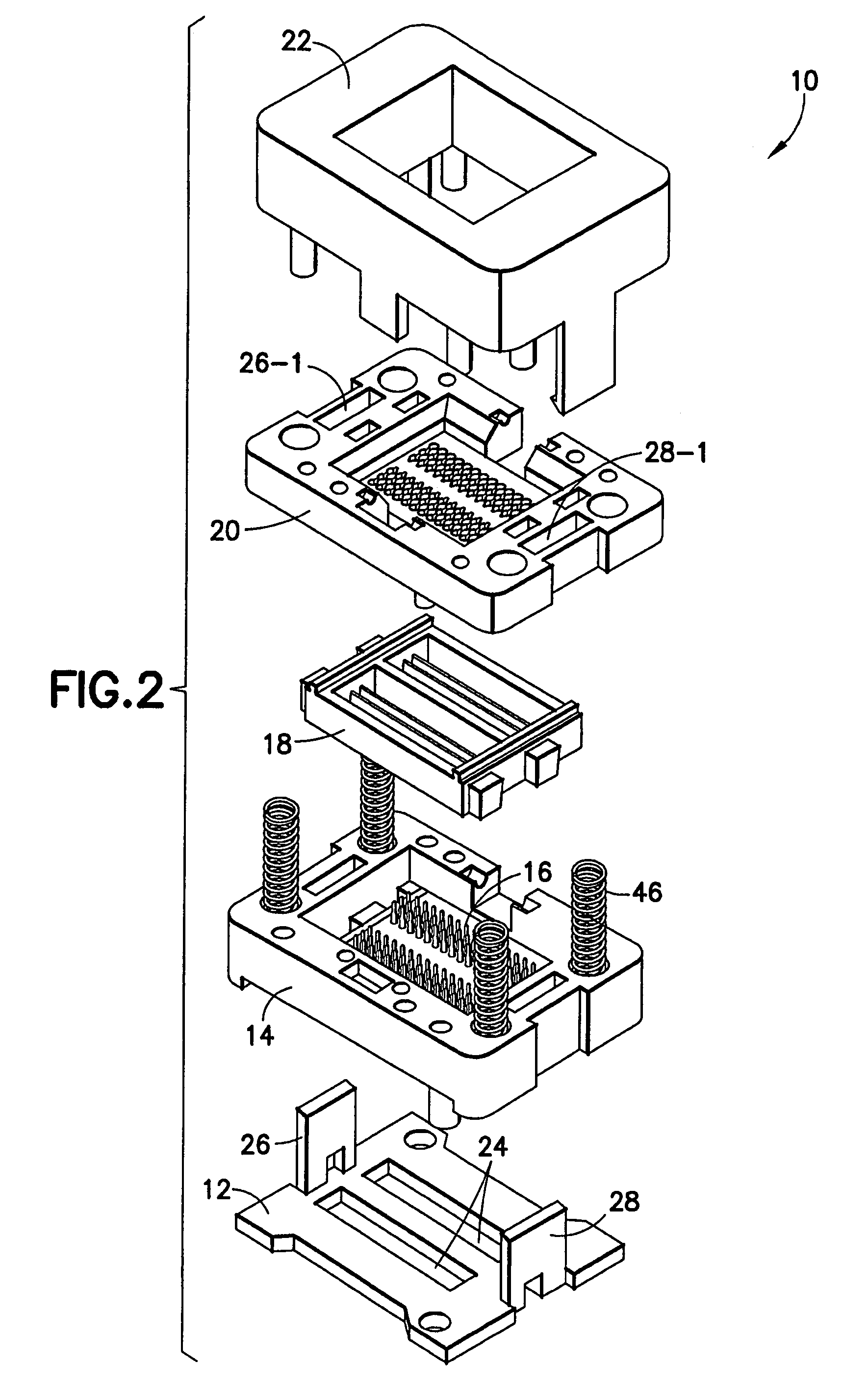
[0047]Referring to FIG. 2, a top loaded, burn-in socket of the present disclosure is generally designated by the numeral 10. The socket 10 includes a base plate or bottom 12 having openings 24 for coupling the socket to a printed circuit board (PCB), an electrical component or the like, a generally rectangular housing 14 having a plurality of apertures, a plurality of resilient electrical contacts 16 disposed in the plurality of apertures and a cam 18 having a plurality of openings corresponding to the plurality of contacts 16...


PUM


Abstract

A top loaded burn-in socket for forming a plurality of electrical connections between a ball gird array (BGA) package having a plurality of conductive ball leads and an electrical component is provided. The socket assembly includes a plurality of resilient electrical contacts; a cam being configured to position the contacts from a first position to a second position; a device guide plate including a plurality of openings for receiving the ball leads; and an actuating mechanism configured to interact with the cam to position the contacts, wherein an upper portion of the contacts engages the ball leads between the upper portion and an inclined surface of the device guide plate openings. Each ball is thus held in a manner that does not require the use of a hold down mechanism for effecting electrical continuity between the BGA package and the contacts of the subject burn-in socket.

Description

PRIORITY[0001]This application claims priority to an application entitled “TOP LOADED BURN-IN SOCKET” filed in the United States Patent and Trademark Office on Aug. 27, 2004 and assigned U.S. Ser. No. 60 / 605,321, the contents of which are hereby incorporated by reference.BACKGROUND[0002]1. Field[0003]The present disclosure relates to a universal burn-in ball grid array socket, and more particularly, a top loaded burn-in socket which eliminates the need for hold down devices when the ball grid array package is inserted into the subject socket.[0004]2. Description of the Related Art[0005]Integrated circuits are typically housed within a package which is designed to protect the integrated circuit from damage, provide adequate heat dissipation during operation, and provide electrical connection between the integrated circuit and the leads of a printed circuit board. Several conventional packages are in the prior art including land grid array (LGA), pin grid array (PGA), ball grid array ...

Claims


Application Information

Patent Timeline
Patent Type & Authority Patents(United States)
IPC IPC(8): H01R11/22
CPCG01R1/0466H01R13/193
Inventor SINCLAIR, WILLIAM Y.
Owner ARIES ELECTRONICS
Why Eureka
Try Eureka