Semiconductor device having a leading wiring layer

Inactive Publication Date: 2006-08-15
SHARP KK
View PDF24 Cites 43 Cited by
  • Summary
  • Abstract
  • Description
  • Claims
  • Application Information

AI Technical Summary

Benefits of technology

[0027]The object of the present invention is to provide a semiconductor device having high reliability and a manufacturing method thereof, by surely (a) preventing electromigration of the leading wiring layer and the insulation layer, and (b) maintaining adhesion of the leading wiring

Problems solved by technology

However, in the conventional arrangement, as shown in FIG. 7, exposure of side surfaces of the main conductor layer 106 causes a problem that electromigration occurs with the second insulation layer 109 on side surfaces of the leading wiring layer 11

Method used


Image

  • Semiconductor device having a leading wiring layer
  • Semiconductor device having a leading wiring layer
  • Semiconductor device having a leading wiring layer

Examples


Example

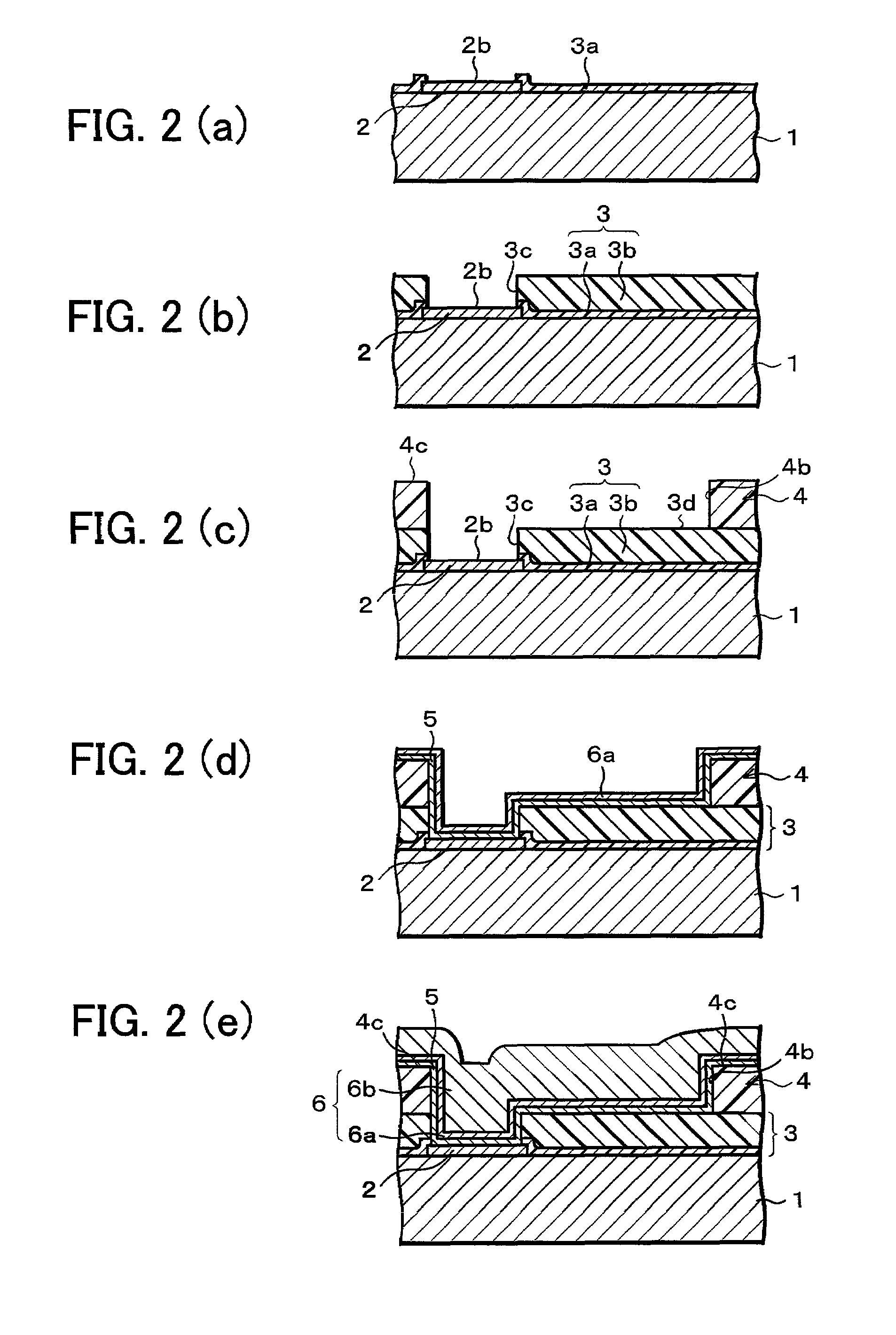
[0043]An embodiment of the present invention is explained as follows, referring to FIGS. 1 through 6.

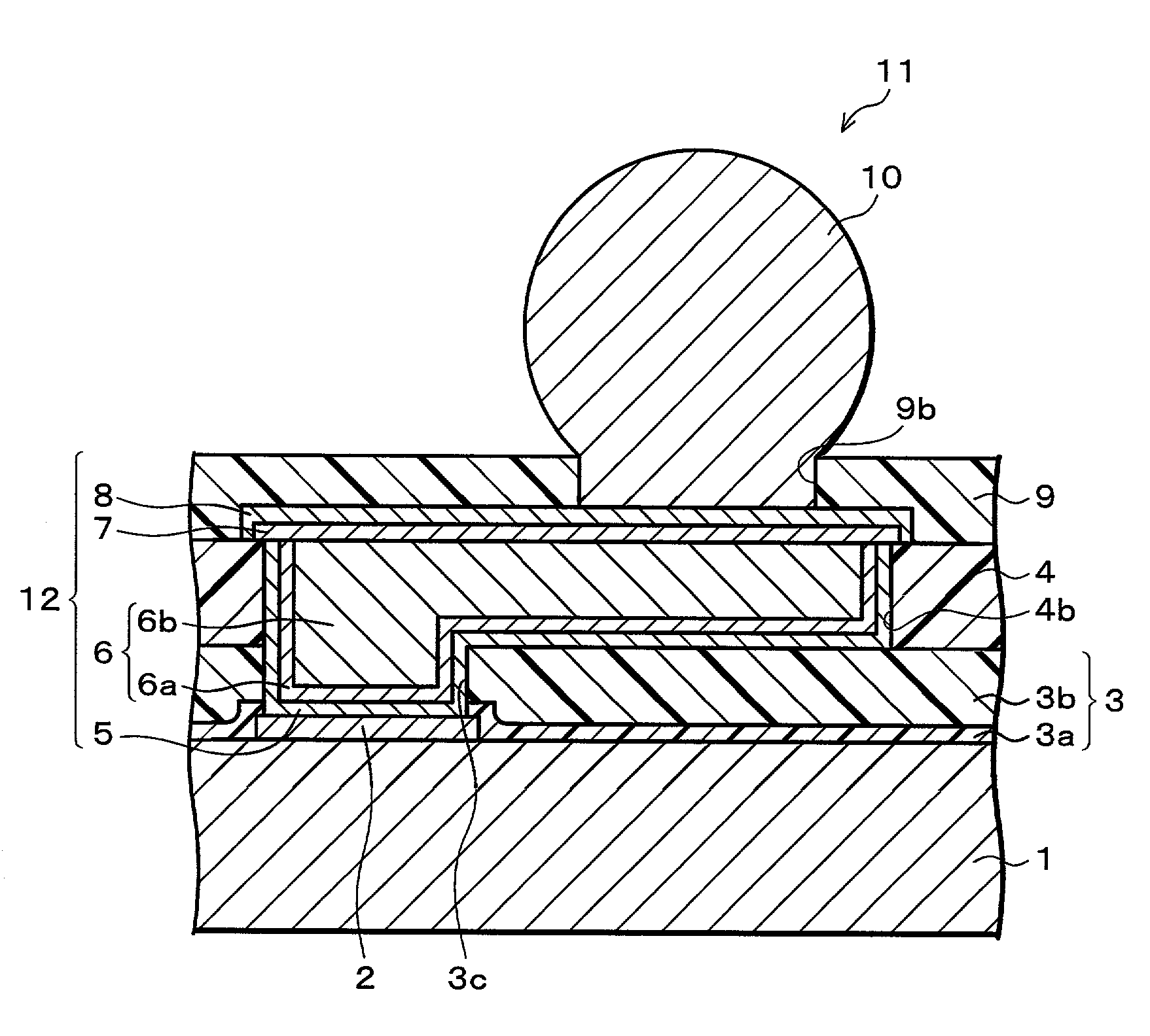
[0044]FIG. 1 shows a cross sectional structure of a main part in a semiconductor device 11 in accordance with the embodiment of the present invention.

[0045]As shown in FIG. 1, the semiconductor device 11 is provided with a semiconductor substrate 1, a plurality of electrode pads 2, a first insulation layer 3, a second insulation layer 4, a leading wiring layer 12, a third insulation layer 9, and a plurality of external connecting terminals 10.

[0046]The plurality of electrode pads 2 and the first insulation layer 3 having a first opening section 3c in an area of the electrode pads 2 are formed on the semiconductor substrate 1. The first insulation layer 3 is composed of an inorganic insulation layer 3a and an organic insulation layer 3b formed on the inorganic insulation layer 3a.

[0047]The leading wiring layer 12 is formed on the electrode pad 2 and the first insulation layer 3. The ...


PUM


Abstract

A leading wiring layer is provided with a main conductor layer, a first barrier metal layer for covering bottom and side surfaces of the main conductor layer, and a second barrier metal layer for covering a top surface of the main conductor layer. This ensures the respective barrier metal layers to cover entire surroundings including the side, bottom and top surfaces of the main conductor layer.

Description

FIELD OF THE INVENTION[0001]The present invention relates to a semiconductor device in which an external connecting terminal and an electrode pad formed on a semiconductor substrate are connected via a leading wiring layer and to its manufacturing method.BACKGROUND OF THE INVENTION[0002]Nowadays, as electronic devices are getting smaller in size and lighter in weight, as represented by a portable device or a mobile device, a semiconductor package used for them is also required to be smaller in size and lighter in weight.[0003]In order to satisfy the demand, a semiconductor package having approximately the same size as a semiconductor chip (hereinafter referred to as a chip), namely a CSP (Chip Size Package) appears and comes into practical use.[0004]Now, the mainstream form of the CSP is a face-up structure using a wire bonding technique. In the CSP, however, after mounting the chip on a substrate called as an interposer, wire bonding is carried out between a wire bonding terminal o...

Claims


Application Information

Patent Timeline
IPC IPC(8): H01L23/48H01L23/52H01L21/3205H01L21/60H01L23/31H01L23/485H01L31/00
CPCH01L23/3114H01L24/10H01L24/13H01L24/05H01L2924/0002H01L2924/01068H01L2224/0231H01L2224/0401H01L2224/05006H01L2224/05546H01L2224/05567H01L2224/13007H01L2224/13022H01L2224/13099H01L2924/01004H01L2924/01005H01L2924/01006H01L2924/01007H01L2924/01013H01L2924/01014H01L2924/01022H01L2924/01027H01L2924/01028H01L2924/01029H01L2924/01046H01L2924/01047H01L2924/0105H01L2924/01074H01L2924/01078H01L2924/01079H01L2924/01082H01L2924/01322H01L2924/014H01L2924/12044H01L2924/01024H01L2924/01033H01L2924/00H01L2224/05552H01L2224/13H01L2224/13024
Inventor SUMINOE, SHINJINAKANISHI, HIROYUKIISHIO, TOSHIYAIWAZAKI, YOSHIHIDEMORI, KATSUNOBU
Owner SHARP KK
Why Eureka
Try Eureka