Multi-chip semiconductor package and fabrication method thereof

a technology of semiconductor packages and fabrication methods, applied in semiconductor devices, semiconductor/solid-state device details, electrical apparatus, etc., can solve problems such as significant problems, adversely affect the reliability of fabricated package products, and the chip size limitation of multi-chip semiconductor packages, so as to reduce the overall package thickness, reduce thermal stress, and improve mechanical strength

Inactive Publication Date: 2006-08-15
UTAC HEADQUARTERS PTE LTD
View PDF2 Cites 23 Cited by
  • Summary
  • Abstract
  • Description
  • Claims
  • Application Information

AI Technical Summary

Benefits of technology

[0007]An objective of the present invention is to provide a multi-chip semiconductor package and a fabrication method thereof, which can prevent a chip accommodated in the semiconductor package from cracking during fabrication processes.
[0008]Another objective of the invention is to provide a multi-chip semiconductor package and a fabrication method thereof, wherein no gap is formed between a non-conductive material and a chip applied with the non-conductive material, such that no void or popcorn effect issue is generated.
[0009]A further objective of the invention is to provide a multi-chip semiconductor package and a fabrication method thereof, which can enhance mechanical strength for a chip and help minish thermal stress exerted to the chip, and also, the chip can be further thinned in favor of reducing overall package thickness.
[0010]A further objective of the invention is to provide a multi-chip semiconductor package and a fabrication method thereof, wherein a non-conductive material is applied over a chip and helps prevent external moisture from invading the chip, thereby assuring reliability of the semiconductor package.
[0013]The above semiconductor package provides significant benefits. First, as the second chip is completely supported on the non-conductive material, during a wire-bonding process for forming the second bonding wires, the suspending portion of the second chip can be prevented from cracking in response to wire-bonding force exerted by a wire bonder, thereby assuring structural intactness of the second chip. Further, as the non-conductive material is directly applied over the first chip without forming gaps therebetween, no void or popcorn effect issue is concerned in this invention for fabricating the encapsulant. Moreover, the second chip is attached with one side thereof to the non-conductive material such as an elastic adhesive, and encapsulated with its opposed side by the encapsulant; this double-side encapsulation enhances mechanical strength and provides buffer effect for the second chip, and helps reduce thermal stress exerted to the second chip during subsequent high-temperature conditions, and also, the second chip can thereby be further thinned in favor of reducing overall package thickness. Furthermore, the non-conductive material applied over the first chip helps prevent external moisture from invading the first chip, thereby assuring reliability of the semiconductor package.

Problems solved by technology

However, this multi-chip semiconductor package 1 is subject to a chip-size limitation problem; that is, the second chip 13 should be smaller in dimension than the first chip 10 so as not to interfere with arrangement of the first bonding wires 12 bonded to the first chip 10.
However, the above multi-chip semiconductor package 1″ in the use of the support members 17, induces significant problems.
During a molding process for forming the chip-encapsulation encapsulant 15 by a resin compound, the relative narrow gaps G would change motion of the resin compound passing therethrough and easily trap air or voids therein; this may lead to popcorn effect with voids left in the encapsulant 15 for the semiconductor package 1″ in subsequent fabrication processes, and thereby adversely affect reliability of fabricated package products.

Method used


Image

  • Multi-chip semiconductor package and fabrication method thereof
  • Multi-chip semiconductor package and fabrication method thereof
  • Multi-chip semiconductor package and fabrication method thereof

Examples


first preferred embodiment

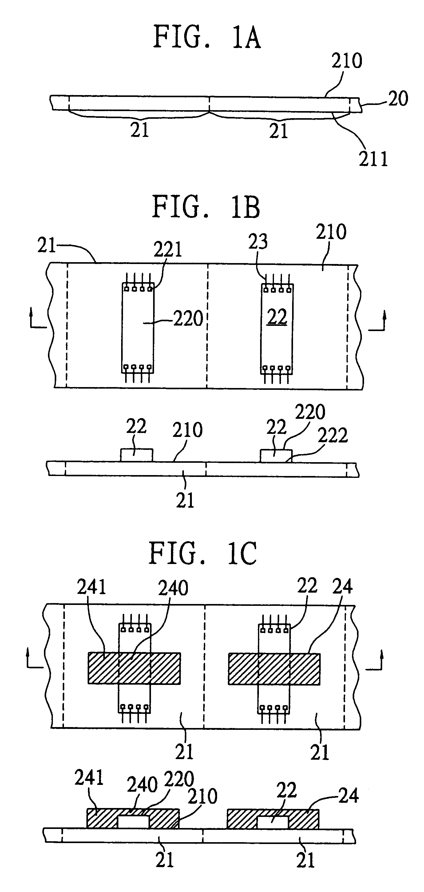
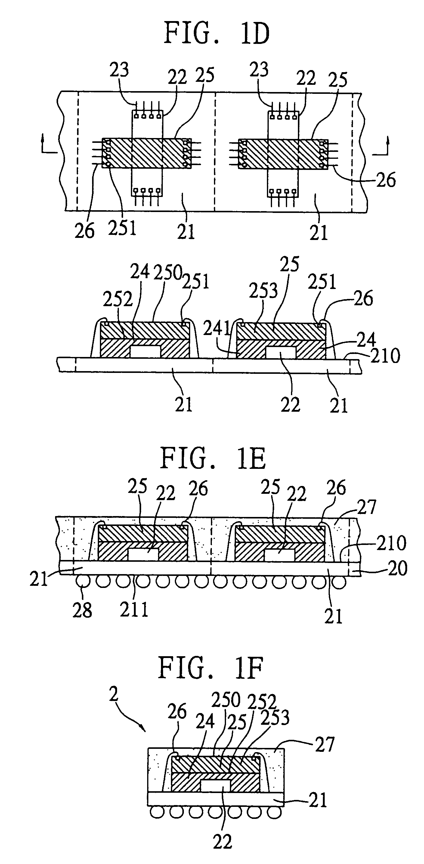
[0022]FIGS. 1A–1F illustrate fabrication processes for a semiconductor package 2 according to a first embodiment of the invention.

[0023]Referring to FIG. 1A, the first step is to prepare a substrate plate 20 integrally formed of a plurality of substrates 21, which are bordered by dotted lines shown in the drawing. Each of the substrates 21 has an upper surface 210 and a lower surface 211 opposed to the upper surface 210. The substrate plate 20 is primarily made of a conventional resin material, such as epoxy resin, polyimide, BT (bismaleimide triazine) resin, FR-4 resin, etc.

[0024]Referring to FIG. 1B, the next step is to mount at least a first chip 22 on the upper surface 210 of each of the substrates 21. The first chip 22 has an active surface 220 where a plurality of electronic elements and circuits (not shown) and bond pads 221 are formed, and a non-active surface 222 opposed to the active surface 220, wherein the non-active surface 222 of the first chip 22 is attached to the up...

second preferred embodiment

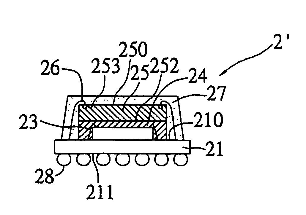
[0033]FIGS. 2A–2D illustrate fabrication processes for a semiconductor package 2′ according to a second preferred embodiment of the invention. This semiconductor package 2′ is structurally similar to the above semiconductor package 2 of the first preferred embodiment; therefore, same components are here designated with same reference numerals as those used in the above first embodiment for easy interpretation and illustration.

[0034]Referring to FIG. 2A, the first step is to prepare a substrate 21 having an upper surface 210 and a lower surface 211 opposed to the upper surface 210. At least a first chip 22 is mounted on the upper surface 210 of the substrate 21; the first chip 22 has an active surface 220 and a non-active surface 222 opposed to the active surface 220, wherein the non-active surface 222 of the first chip 22 is attached to the upper surface 210 of the substrate 21. A plurality of first bonding wires 23 such as gold wires are formed to electrically connect the active su...


PUM


Abstract

A multi-chip semiconductor package and a fabrication method thereof are provided. A substrate having an upper surface and a lower surface is prepared. At least a first chip is mounted on the upper surface of the substrate. A non-conductive material is applied over predetermined area on the first chip and the upper surface of the substrate. At least a second chip is mounted on the non-conductive material, and formed with at least a suspending portion free of interference in position with the first chip, wherein the non-conductive material is dimensioned in surface area at least corresponding to the second chip, so as to allow the suspending portion to be supported on the non-conductive material. With the second chip being completely supported on the non-conductive material without causing a conventional chip-crack problem, structural intactness and reliability can be effectively assured for fabricated package products.

Description

CROSS REFERENCE TO RELATED APPLICATIONS[0001]This application is a divisional application of U.S. patent application Ser. No. 10 / 261,796, filed on Sep. 30, 2002 U.S. Pat. No. 6,825,064, which is incorporated herein by reference.FIELD OF THE INVENTION[0002]The present invention relates to multi-chip semiconductor packages, and more particularly, to a semiconductor package with a plurality of chips mounted on a chip carrier, and a fabrication method of the semiconductor package.BACKGROUND OF THE INVENTION[0003]In favor of effective enhancement in electrical and operational performances, it preferably incorporates more than one or a plurality of chips in a single package, thus forming a multi-chip semiconductor package. A conventional multi-chip semiconductor package 1, as shown in FIG. 3, is a substrate-based structure, wherein a first chip 10 is mounted on a substrate 11 and electrically connected thereto by a plurality of first bonding wires 12. A second chip 13 is stacked on the fi...

Claims


Application Information

Patent Timeline
Patent Type & Authority Patents(United States)
IPC IPC(8): H01L23/48H01L23/52H01L21/44H01L21/50H01L21/98H01L25/065H01L29/768
CPCH01L24/97H01L25/0657H01L25/50H01L2224/45144H01L2924/01087H01L2924/01033H01L2924/01082H01L2924/01079H01L2225/06582H01L2225/06575H01L2224/48091H01L2224/48227H01L2224/97H01L2225/0651H01L2225/06555H01L2225/06562H01L2924/00014H01L2224/83H01L2224/85H01L2924/00H01L2924/351
Inventor TSAI, SHIANN-TSONGHSU, YU-MINGWU, WEN-LUNGCHEN, KUEN-HUANGSU, WEN-SHENGLIN, CHIN-HSING
Owner UTAC HEADQUARTERS PTE LTD
Why Eureka
Try Eureka