System and method for determining on-chip bit error rate (BER) in a communication system

a communication system and bit error rate technology, applied in the field of optical networking hardware, can solve the problems of difficult testing of optical transceivers, ber testing by applying input signals and capturing outputs by external devices, and defective links or devices comprising links may be detected

Inactive Publication Date: 2006-08-15
AVAGO TECH INT SALES PTE LTD
View PDF13 Cites 50 Cited by
  • Summary
  • Abstract
  • Description
  • Claims
  • Application Information

AI Technical Summary

Benefits of technology

[0016]Further limitations and disadvantages of conventional and traditional approaches will become apparent to one of skill in the art, through comparison of such systems with the present invention as set forth in the remainder of the present application with reference to the drawings.

Problems solved by technology

In this regard, defective links or devices comprising the links may be detected when the captured output signals are inconsistent with the expected outputs.
Testing BER for a communication link by applying input signals and capturing of outputs by an external device may become difficult as the data rate of the communication links increase.
Testing optical transceivers may be challenging because of the high speeds at which these devices operate.

Method used


Image

  • System and method for determining on-chip bit error rate (BER) in a communication system
  • System and method for determining on-chip bit error rate (BER) in a communication system
  • System and method for determining on-chip bit error rate (BER) in a communication system

Examples


Embodiment Construction

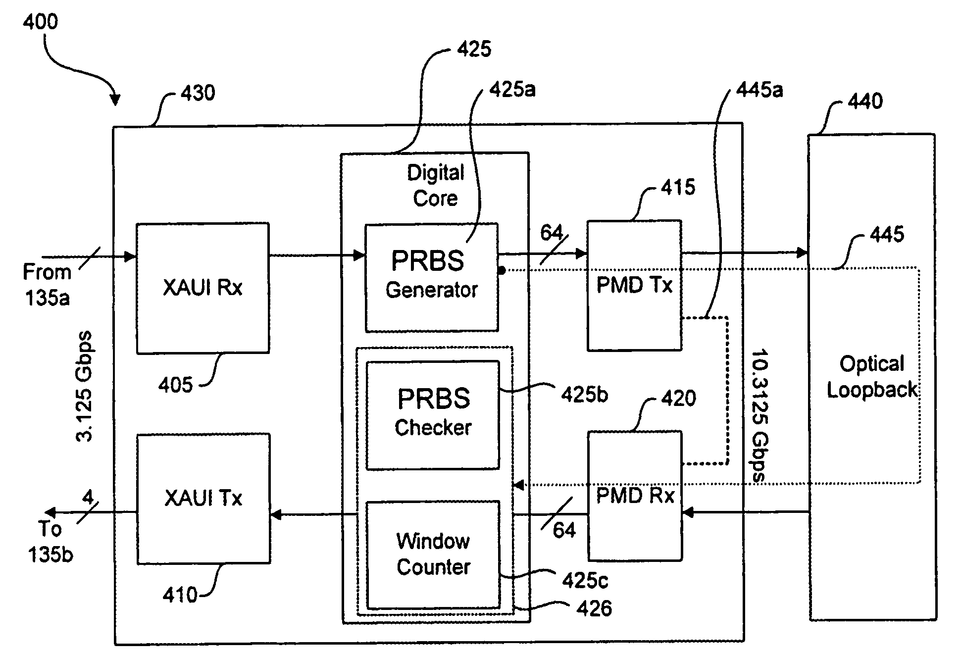
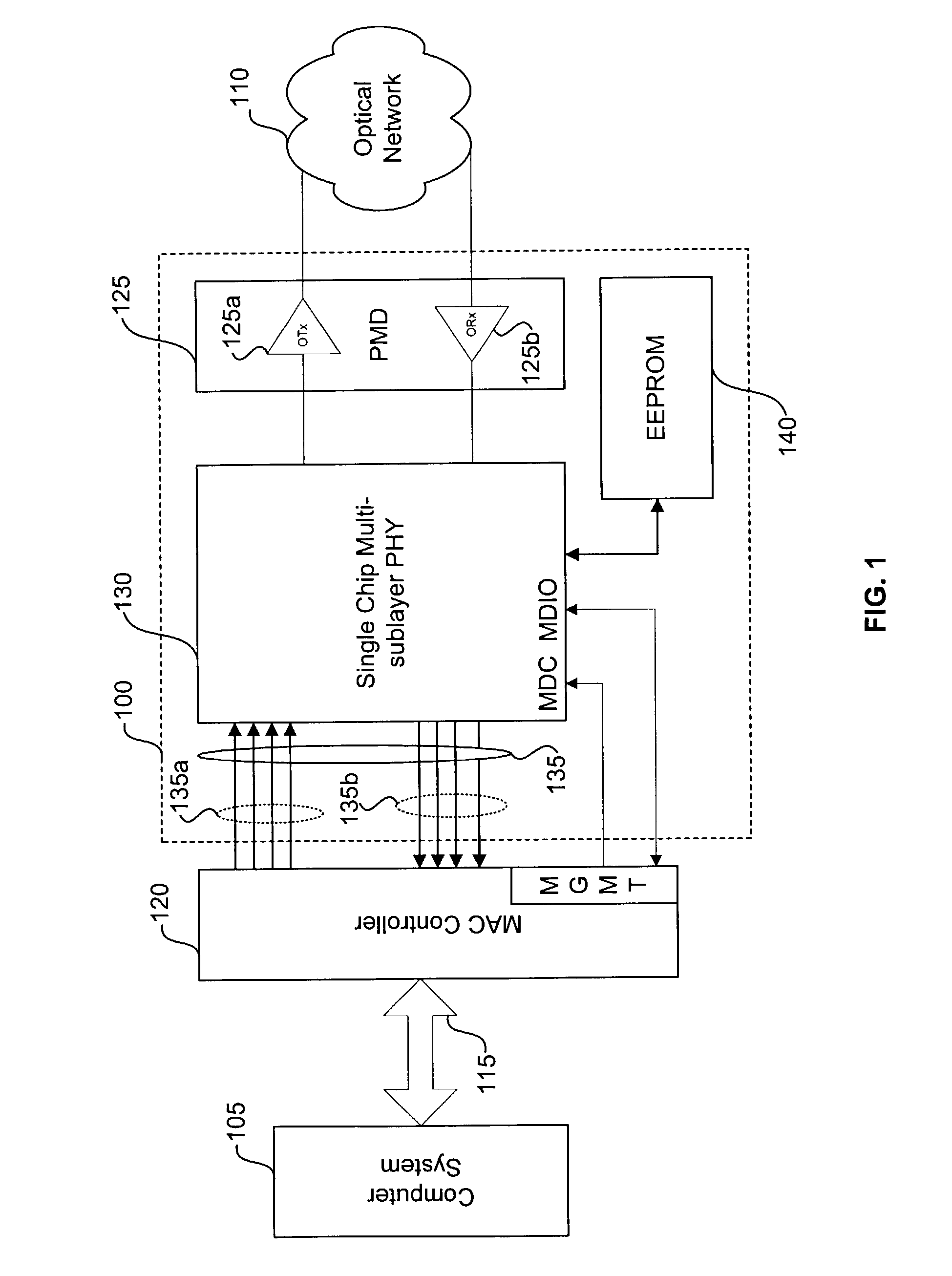
[0044]FIG. 1 is a block diagram of an exemplary transceiver module 100 in accordance with one aspect of the invention. Referring to FIG. 1, there is also illustrated a computer system 105, a MAC controller 120, a MAC controller interface 115, an optical network 110, a single-chip multimode multi-sublayer PHY device 130, an electrically erasable programmable read only memory (EEPROM) 140, an PMD transmitter 125a and an PMD receiver 125b. PMD transmitter 125a and PMD receiver 125b may be integrated into a single PMD 125 such as a chip or IC, although the invention is not limited in this regard. Transceiver module 100 may be an integrated device, which may include the single-chip multimode multi-sublayer PHY device 130, the EEPROM 140, the optical transmitter 125a and the optical receiver 125b. Computer system 105 may interface with MAC controller 120 through the medium access controller interface 115 and may communicate with the optical network 110 through the transceiver module 100.

[...


PUM


Abstract

A test packet generator (225a) within a physical layer device (230) may generate test packets to be communicated over a closed communication path established within the physical layer device (230). The test packets may include a pseudo-random bit sequence. A receiver within the physical layer device (230) may receive at least a portion of the generated test packet. A test packet checker (225b) within the physical layer device may compare at least a portion of the received test packets with at least a portion of the generated test packets in order to determine the bit error rate for the physical layer device. A window counter (225c) within the physical layer device (230) may count at least a portion of a number of bits received within the generated test packets and a number of bits that are in error in at least a portion of the number of bits received. Accordingly, the bit error rate may be calculated based on a ratio of the number of counted bits in error to the number bits counted in the at least a portion of the number of bits received.

Description

CROSS-REFERENCE TO RELATED APPLICATIONS / INCORPORATION BY REFERENCE[0001]This application makes reference to, claims priority to and claims the benefit of U.S. Provisional Patent Application Ser. No. 60 / 402,094 filed on Aug. 7, 2002.[0002]This application also makes reference to U.S. Pat. No. 6,424,194, U.S. application Ser. No. 09 / 540,243 filed on Mar. 31, 2000, U.S. Pat. No. 6,389,092, U.S. Pat. No. 6,340,899, U.S. application Ser. No. 09 / 919,636 filed on Jul. 31, 2001, U.S. application Ser. No. 09 / 860,284 filed on May 18, 2001, U.S. application Ser. No. 10 / 028,806 filed on Oct. 25, 2001, U.S. application Ser. No. 09 / 969,837 filed on Oct. 1, 2001, U.S. application Ser. No. 10 / 159,788 entitled “Phase Adjustment in High Speed CDR Using Current DAC” filed on May 30, 2002, U.S. application Ser. No. 10 / 179,735 entitled “Universal Single-Ended Parallel Bus; fka, Using 1.8V Power Supply in 0.13 MM CMOS” filed on Jun. 21, 2002, and U.S. application Ser. No. 60 / 402,090 entitled “System and ...

Claims


Application Information

Patent Timeline
Patent Type & Authority Patents(United States)
IPC IPC(8): G01R31/28H04L12/26H04L5/16H04L1/20H04L1/24
CPCH04L1/241H04L1/203H04L1/243
Inventor FAN, NONGHOANG, TUANJIANG, HONGTAO
Owner AVAGO TECH INT SALES PTE LTD
Why Eureka
Try Eureka